Introduction
This chapter provides an overview of the Realtek DMAC, which transmits data from the source to the destination through the AXI bus.
General Description
The following figure shows the following functional groupings of the main interfaces to the RTK_DMAC block:
DMA hardware request interface
Up to sixteen channels, the specific number is subject to the IP configuration form.
FIFO per channel for source and destination
Arbiter
AXI master interface
APB slave interface
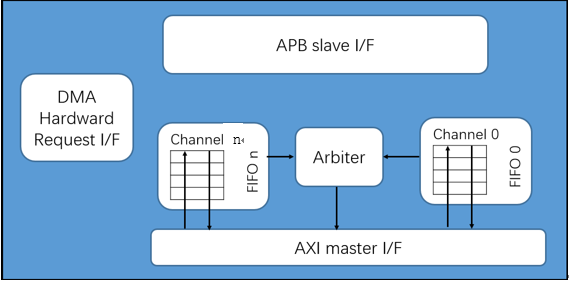
Block diagram of DMAC
One channel of the RTK_DMAC is required for each source/destination pair. In the most basic configurations, the RTK_DMAC has one AXI master interface (two AXI transfers) and one channel. The master interfaces reads the data from a source peripheral (A) and writes it to a destination peripheral (B). Two AXI transfers are required for each DMA data transfer; this is also known as a dual-access transfer.
Basic Definitions
The following terms are concise definitions of the DMA concepts used throughout this data book:
Source peripheral – Device from which the RTK_DMAC reads data; the RTK_DMAC then stores the data in the channel FIFO. The source peripheral teams up with a destination peripheral to form a channel. The source peripheral is generally AXI slave.
Destination peripheral – Device to which the RTK_DMAC writes the stored data from the FIFO (previously read from the source peripheral). The destination peripheral is AXI slave.
Memory – Source or destination that is always ready for a DMA transfer and does not require a handshaking interface to interact with the RTK_DMAC.
Channel – Read/write data path between a source peripheral on one configured AXI layer and a destination peripheral on the same or different AXI layer that occurs through the channel FIFO. If the source peripheral is not a memory, then a source handshaking interface is assigned to the channel. If the destination peripheral is not a memory, then a destination handshaking interface is assigned to the channel. Source and destination handshaking interfaces can be assigned dynamically by programming the channel registers.
Master interface – RTK_DMAC is a master on the AXI bus, reading data from the source and writing it to the destination over the AXI bus.
Slave interface – The APB interface over which the RTK_DMAC is programmed.
Handshaking interface – A set of handshake signals that conforms to a protocol between the RTK_DMAC and source/destination peripheral are used to control transferring a single or burst transaction between them. This interface is used to request, acknowledge, and control a RTK_DMAC transaction. A channel can receive a request through these handshaking interface: hardware or peripheral interrupt.
Hardware handshaking interface – Uses hardware signals to control transferring a single or burst transaction between the RTK_DMAC and the source or destination peripheral. For more information about this interface, refer to “Hardware Handshaking – Peripheral Is Not Flow Controller” and “Hardware Handshaking – Peripheral Is Flow Controller” (not supported).
Peripheral interrupt handshaking interface – Simple use of the hardware handshaking interface. In this mode, the interrupt line from the peripheral is tied to the dma_req input of the hardware handshaking interface; other interface signals are ignored.
Flow controller – Device (either the RTK_DMAC, or source/destination peripheral) that determines the length of a DMA block transfer and terminates it.
If you know the length of a block before enabling the channel, then you should program the RTK_DMAC as the flow controller.
If the length of a block is not known prior to enabling the channel, the source or destination peripheral needs to terminate a block transfer. In this mode, the peripheral is the flow controller.
Flow control mode (CFGx.FCMODE) – Special mode that only applies when the destination peripheral is the flow controller. It controls the data pre-fetching from the source peripheral.
Block – Block of RTK_DMAC data, the amount of which is the block length and is determined by the flow controller. For transfers between the RTK_DMAC and memory, a block is broken directly into a sequence of bursts (including burst length = 1).
Transaction – Basic unit of a RTK_DMAC transfer, as determined by the hardware. A transaction is relevant only for transfers between the RTK_DMAC and a source/destination peripheral if the peripheral is a non-memory There are two types of transactions:
Single transaction – Length of a single transaction is always 1 and is converted to a single AXI transfer.
Burst transaction – Length of a burst transaction is programmed into the RTK_DMAC. The burst transaction is converted into a sequence of bursts and AXI single transfers. RTK_DMAC executes each burst transfer by performing incremental bursts that are no longer than the maximum burst size set; the only type of AXI burst in this kind of transaction is incremental. The burst transaction length is under program control and normally bears some relationship to the FIFO sizes in the RTK_DMAC and in the source and destination peripherals.
DMA transfer – Software controls the number of blocks in a RTK_DMAC transfer. Once the DMA transfer has completed, the hardware within the RTK_DMAC disables the channel and can generate an interrupt to signal the DMA transfer completion. You can then reprogram the channel for a new DMA transfer.
Single-block DMA transfer – Consists of a single block.
Multi-block DMA transfer – DMA transfer may consist of multiple RTK_DMAC blocks.
Multi-block DMA transfers are supported through block chaining (linked list pointers), auto-reloading channel registers, and contiguous blocks. The source and destination can independently select which method to use.
Linked lists (block chaining) – Linked list pointer (LLP) points to the location in system memory where the next linked list item (LLI) exists. The LLI is a set of registers that describes the next block (block descriptor) and an LLP register. The RTK_DMAC fetches the LLI at the beginning of every block when block chaining is enabled. For more information about linked lists and block chaining, refer to “Block Chaining Using Linked Lists”.
LLI accesses are always 32-bit accesses (axsize = 2) aligned to 32-bit boundaries and cannot be changed or programmed to anything other than 32-bit.
Auto-reloading – RTK_DMAC automatically reloads the channel registers at the end of each block to the value when the channel was first enabled. For more information about this function, refer to “Auto-Reloading of Channel Registers”
Contiguous blocks – Address between successive blocks is selected to be a continuation from the end of the previous block. For more information, refer to “Contiguous Address between Blocks”.
Scatter – Relevant to destination transfers within a block. The destination address is incremented or decremented by a programmed amount when a scatter boundary is reached. The number of AXI transfers between successive scatter boundaries is under software control.
Gather – Relevant to source transfers within a block. The source address is incremented or decremented by a programmed amount when a gather boundary is reached. The number of AXI transfers between successive gather boundaries is under software control.
For more information about scatter and gather, refer to “Scatter/Gather”.
备注
Not support unaligned Scatter & Gather in current version.
FIFO mode – Special mode to improve bandwidth. When enabled, the channel waits until the FIFO is less than half full to fetch the data from the source peripheral, and waits until the FIFO is greater than or equal to half full in order to send data to the destination peripheral. Because of this, the channel can transfer the data using bursts, which eliminates the need to arbitrate for the AXI master interface in each single AXI transfer. When this mode is not enabled, the channel waits only until the FIFO can transmit or accept a single AXI transfer before it requests the master bus interface.
Features
The DMAC component includes the following features.
General
AXI-4 compliant
APB4 slave interface is used to program registers.
AXI master interface
Configurable data bus width (32bits) for AXI master interface
Configurable endianness for master interfaces
Channels
Up to eight channels
Unidirectional channels – data transfers in one direction only
Programmable channel priority
Transfers: support for memory-to-memory, memory-to-peripheral, peripheral-to-memory, and peripheral-to-peripheral DMA transfers
Secure mode support: channels can be configured to secure mode to enhance the security
Power save: support DMAC low power mode (internal clock gating)
FIFO per channel for source and destination, the FIFO depth for channel 0/1 is 128 bytes, while 32 bytes for other channels.
Transaction
Size: the max. transfer size for one block is 2097151.
Mode: support single block mode and multi-block mode.
Type: Support memory-to-memory, memory-to-peripheral, peripheral-to-memory, and peripheral-to-peripheral.
All synchronous design (only 1 clock)
Address Generation
Programmable source and destination addresses (on AXI bus)
Address increment, or no change
Multi-block transfers achieved through:
Linked Lists (block chaining)
Auto-reloading of channel registers
Contiguous address between blocks
Independent source and destination selection of multi-block transfer type
Scatter/Gather
Channel Buffering
Single FIFO per channel for source and destination
FIFO depth: The FIFO depth of channel 0 and 1 is 128bytes, and the remaining channels are 32bytes
D flip-flop-based FIFO
Channel Control
Programmable source and destination for each channel
Programmable transfer type for each channel (memory-to-memory, memory-to-peripheral, peripheral-to-memory, and peripheral-to-peripheral)
Programmable burst transaction size for each channel
Programmable enable and disable of DMA channel
Support for disabling channel without data loss
Support for suspension of DMA operation
Support for ERROR responses
Programmable maximum burst transfer size per channel
Configurable maximum transaction size to allow gate optimization
Configurable maximum block size to allow gate optimization
Option to disable the write-back of the Channel Control register at the end of every block transfer
Transfer Initiation
Handshaking interfaces for source and destination peripherals (up to 128)
Hardware handshaking interface
Peripheral interrupt handshaking interface (not support now)
以下内容待确定
UART0 Tx/Rx
UART1 Tx/Rx
UART2 Tx/Rx
SPI0 Tx/Rx
SPI1 Tx/Rx
SPIC Tx/Rx
SPORT0F0 Tx/Rx
SPORT0F1 Tx/Rx
SPORT1F0 Tx/Rx
SPORT1F1 Tx/Rx
LEDC Tx
I2C0 Tx/Rx
I2C1 Tx/Rx
Handshaking interface supports single or burst DMA transactions
Polarity control for hardware handshaking interface
Enabling and disabling of individual DMA handshaking interfaces
Flow Control
Programmable flow control at block transfer level
Software control of source data pre-fetch when destination is flow controller
Interrupts
Combined and separate interrupt requests
Interrupt generation on:
DMA transfer (multi-block) completion
Block transfer completion (contains block and block transfer completion)
Error condition (contain secure error and protocol error)
Support of interrupt enabling and masking
Secure Mode
Secure control bit in configure register
Secure access for master interface and slave interface when secure bit set.
Functional Description
This section describes the functional details of the DMAC component.
Block Flow Controller and Transfer Type
The device that controls the length of a block is known as the flow controller. Either the DMAC, the source peripheral, or the destination peripheral must be assigned as the flow controller.
If the block size is known prior to when the channel is enabled, then the DMAC should be programmed as the flow controller. The block size should be programmed into the CTLx.BLOCK_TS field.
If the block size is unknown when the DMAC channel is enabled, either the source or destination peripheral must be the flow controller.
The CTLx.TT_FC field indicates the transfer type and flow controller for that channel. The following table lists valid transfer types and flow controller combinations.
Transfer type |
Flow controller |
|---|---|
Memory to Memory |
DMAC |
Memory to Peripheral |
DMAC |
Memory to Peripheral |
Peripheral |
Peripheral to Memory |
DMAC |
Peripheral to Memory |
Peripheral |
Peripheral to Peripheral |
DMAC |
Peripheral to Peripheral |
Source Peripheral |
Peripheral to Peripheral |
Destination Peripheral |
As an example, the DMAC can be programmed as the flow controller when a DMA block must be transferred from a receive peripheral to memory. Software then programs the CTLx.BLOCK_TS register with the same value and programs the DMAC as the flow controller.
Handshaking Interface
Handshaking interfaces are used at the transaction level to control the flow of single or burst transactions. The operation of the handshaking interface is different and depends on whether the peripheral or the DMAC is the flow controller.
The peripheral uses the handshaking interface to indicate to the DMAC that it is ready to transfer or accept data over the bus.
A non-memory peripheral can request a DMA transfer through the DMAC using hardware handshaking interfaces.
备注
Throughout the remainder of this document, references to both source and destination hardware handshaking interfaces assume an active-high interface (refer to CFGx.SRC(DST)_HS_POL bits in the Channel Configuration register). When active-low handshaking interfaces are used, then the active level and edge are reversed from that of an active-high interface.
The type of handshaking interface depends on whether the peripheral is a flow controller or not.
备注
Source and destination peripherals can independently select the handshaking interface type. For more information, refer to the CFGx.HS_SEL_SRC and CFGx.HS_SEL_DST parameters in the CFGx register.
Memory Peripherals
For memory, there is no handshaking interface with the DMAC, and therefore the memory peripheral can never be a flow controller. Once the channel is enabled, the transfer proceeds immediately without waiting for a transaction request.
Basic Interface Definitions
The following definitions are used in a data transaction.
Source single transaction size in bytes
src_single_size_bytes = CTLx.SRC_TR_WIDTH/8
Source burst transaction size in bytes
src_burst_size_bytes = CTLx.SRC_MSIZE * src_single_size_bytes
Destination single transaction size in bytes
dst_single_size_bytes = CTLx.DST_TR_WIDTH/8
Destination burst transaction size in bytes
dst_burst_size_bytes = CTLx.DST_MSIZE * dst_single_size_bytes
Block size in bytes
DMAC is flow controller–With the DMAC as the flow controller, the processor programs the DMAC with the number of data items (block size) of source transfer width (CTLx.SRC_TR_WIDTH) to be transferred by the DMAC in a block transfer; this is programmed into the CTLx.BLOCK_TS field. Therefore, the total number of bytes to be transferred in a block is:
blk_size_bytes_dma = CTLx.BLOCK_TS * src_single_size_bytes
Source peripheral is block flow controller
blk_size_bytes_src = (Number of source burst transactions * src_burst_size_bytes) + (Number of source single transactions * src_single_size_bytes)
Destination peripheral is block flow controller
blk_size_bytes_dst = (Number of destination burst transactions * dst_burst_size_bytes) + (Number of destination single transactions * dst_single_size_bytes)
Setting up Transfers
Transfers are set up by programming fields of the CTLx and CFGx registers for that channel. A single block is made up of numerous transactions – single and burst – which are in turn composed of OCP transfers. A peripheral requests a transaction through the handshaking interface to the DMAC. The operation of the handshaking interface is different and depends on what is acting as the flow controller.
The following table lists the parameters that are investigated in a transaction.
Parameter |
Description |
|---|---|
DMAC_CHx_FIFO_DEPTH |
Channel x FIFO depth in bytes, 128 bytes for channel 0/1, while 32 bytes for others |
CTLx.TT_FC |
Transfer type and flow control |
CTLx.BLOCK_TS |
Block transfer size |
CTLx.SRC_TR_WIDTH |
Source transfer width |
CTLx.DST_TR_WIDTH |
Destination transfer width |
CTLx.SRC_MSIZE |
Source burst transaction length |
CTLx.DEST_MSIZE |
Destination burst transaction length |
CFGx.FIFO_MODE |
FIFO mode select |
CFGx.FCMODE |
Flow-control mode |
Generating Requests for the Master Bus Interface
Each channel has a source state machine and destination state machine running in parallel. These state machines generate the request inputs to the arbiter, which arbitrates for the master bus interface (one arbiter per master bus interface).
When the source/destination state machine is granted control of the master bus interface, and when the master bus interface is granted control of the external bus, then transfers between the peripheral and the DMAC (on behalf of the granted state machine) can take place.
Transfers from the source peripheral or to the destination peripheral cannot proceed until the channel FIFO is ready. For burst transaction requests and for transfers involving memory peripherals, the criterion for “FIFO readiness” is controlled by the FIFO_MODE field of the CFGx register.
The definition of FIFO readiness is the same for:
Single transactions
Burst transactions, where CFGx.FIFO_MODE = 0
Transfers involving memory peripherals, where CFGx.FIFO_MODE = 0
The channel FIFO is deemed ready when the space/data available is sufficient to complete a single transfer of the specified transfer width. FIFO readiness for source transfers occurs when the channel FIFO contains enough room to accept at least a single transfer of CTLx.SRC_TR_WIDTH width. FIFO readiness for destination transfers occurs when the channel FIFO contains data to form at least a single transfer of CTLx.DST_TR_WIDTH width.
备注
An exception to FIFO readiness for destination transfers occurs in “FIFO flush mode.” In this mode, FIFO readiness for destination transfers occurs when the channel FIFO contains data to form at least a single transfer of CTLx.SRC_TR_WIDTH width (and not CTLx.DST_TR_WIDTH width, as is the normal case).
When CFGx.FIFO_MODE = 1, then the criteria for FIFO readiness for burst transaction requests and transfers involving memory peripherals are as follows:
A FIFO is ready for a source burst transfer when the FIFO has enough space for a source burst.
A FIFO is ready for a destination burst transfer when the FIFO is greater than or equal to a destination burst full.
Exceptions to this “readiness” occur. During these exceptions, a value of CTLx.FIFO_MODE = 0 is assumed. The following are the exceptions:
Near the end of a burst transaction or block transfer – The channel source state machine does not wait for the channel FIFO to be less than half empty if the number of source data items left to complete the source burst transaction or source block transfer is less than DMAC_CHx_FIFO_DEPTH/2. Similarly, the channel destination state machine does not wait for the channel FIFO to be greater than or equal to half full, if the number of destination data items left to complete the destination burst transaction or destination block transfer is less than DMAC_CHx_FIFO_DEPTH/2.
In FIFO flush mode
When a channel is suspended – The destination state machine does not wait for the FIFO to become half empty to flush the FIFO, regardless of the value of the FIFO_MODE field.
When the source/destination peripheral is not memory, the source/destination state machine waits for a single/burst transaction request. Upon receipt of a transaction request and only if the channel FIFO is “ready” for source/destination transfers, a request for the master bus interface is made by the source/destination state machine.
备注
There is one exception to this, which occurs when the destination peripheral is the flow controller and CFGx.FCMODE = 1 (data pre-fetching is disabled). Then the source state machine does not generate a request for the master bus interface (even if the FIFO is “ready” for source transfers and has received a source transaction request) until the destination requests new data.
When the source/destination peripheral is memory, the source/destination state machine must wait until the channel FIFO is “ready.” A request is then made for the master bus interface. There is no handshaking mechanism employed between a memory peripheral and the DMAC.
Scatter/Gather
Scatter
Scatter is relevant to a destination transfer. The destination address is incremented by a programmed amount – the scatter increment – when a scatter boundary is reached.
The following figure shows an example destination scatter transfer. The destination address is incremented by the value stored in the destination scatter increment (DSRx_L.DSI) field, multiplied by the number of bytes in a single AXI transfer to the destination (decoded value of CTLx_L.DST_TR_WIDTH)/8 – when a scatter boundary is reached. The number of destination transfers between successive scatter boundaries is programmed into the Destination Scatter Count (DSC) field of the DSRx register.
Scatter is enabled by writing a 1 to the CTLx_L.DST_SCATTER_EN field. The CTLx_L.DINC field determines if the address is incremented or remains fixed. If the CTLx_L.DINC field indicates a fixed-address control throughout a DMA transfer, then the CTLx_L.DST_SCATTER_EN field is ignored, and the scatter feature is automatically disabled.
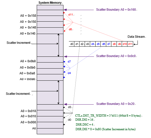
Example of Destination Scatter Transfer
As an example of gather increment, consider the following:
SRC_TR_WIDTH = 3'b 010 (32 bit)
SGRx_L.SGC = 0x04 (source gather count)
CTLx_L.SRC_GATHER_EN = 1 (source gather enabled)
SARx = A0 (starting source address)
Example of Destination Scatter Transfer shows a source gather when SGRx_L.SGI = 0x01.
Gather
Gather is relevant to a source transfer. The source address is incremented or decremented by a programmed amount when a gather boundary is reached.
Example of Destination Scatter Transfer shows an example destination gather transfer. The number of source transfers between successive gather boundaries is programmed into the Source Gather Count (SGRx_L.SGC) field. The source address is incremented or decremented by the value stored in the source gather increment (SGRx_L.SGI) field, multiplied by the number of bytes in a single AXI transfer from the source – (decoded value of CTLx_L.SRC_TR_WIDTH)/8 – when a gather boundary is reached.
Gather is enabled by writing a 1 to the CTLx_L.SRC_GATHER_EN field. The CTLx_L.SINC field determines if the address is incremented, decremented, or remains fixed when a gather boundary is reached. If the CTLx_L.SINC field indicates a fixed-address control throughout a DMA transfer, then the CTLx_L.SRC_GATHER_EN field is ignored, and the gather feature is automatically disabled.
备注
For multi-block transfers, the counters that keep track of the number of transfers left to reach a gather/scatter boundary are re-initialized to the source gather count (SGRx_L.SGC) and destination scatter count (DSC), respectively, at the start of each block transfer.
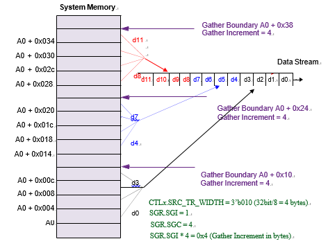
Source Gather when SGRx_L.SGI = 0x1
In general, if the starting address is A0 and CTLx.SINC = 2’b00 (increment source address control), then the transfer will be:
A0, A0 + TWB, A0 + 2*TWB …….(A0 + (SGR.SGC-1)*TWB)
<-scatter_increment-> (A0 + (SGR.SGC*TWB) + (SGR.SGI*TWB))
Where TWB is the transfer width in bytes, decoded value of CTLx.SRC_TR_WIDTH/8 = src_single_size_bytes.
Secure Mode
DMAC supports secure mode, which can prevent non-secure access to secure range. When CPU configures the DMAC transfer without secure mode register access, the secure access bit will not be set. For AXI DMAC, master interface will output AxProt[1] =0 for secure access to source or destination address.
Generally, secure slave will response error data (for source) or reject the write (for destination) when non-secure access to it.
The work flow for secure DMAC transfer should be as follows:
Set the secure access bit to 0 in configure register for some channel with secure mode write.
Enable the DMAC transfer.
Wait for DMAC transfer over or interrupt, then DMAC will clear channel enable bit automatically.
Secure access bit should be cleared when the channel doesn’t need secure access anymore.
Refer to the registers for more details.
Registers
This section describes the programmable registers of the DMAC. All registers are aligned to a 64-bit boundary and are 64 bits wide. In general, the upper 32 bits of a register are reserved. A write to reserved bits within the register is ignored if there is no special explanation.
备注
There are references to both software and hardware parameters throughout this chapter.
The software parameters are the field names in each register description table and are prefixed by the register name; for example, the Block Transfer Size field in the Control register for Channel x is designated as “CTLx.BLOCK_TS.”
The hardware parameters are prefixed with DMAC_* and are configured once using Realtek coreTools.
Shipped with the RTK_DMAC component is an address definition (memory map) C header file. This can be used when the RTK_DMAC is programmed in a C environment
Register Memory Map
The following table shows the memory map for the DMAC.
备注
The address offsets of the registers are always fixed, regardless of the number of configured channels.
Name |
Address offset |
Access |
Reset |
Description |
|---|---|---|---|---|
Channel Registers If DMAC_NUM_CHANNELS = “dnc”, “Reg Exist” field shows “dnc” value for register to exist. |
||||
SAR0 |
0x000 |
R/W |
0x0 |
Channel 0 Source Address Register Reg Exist: Yes |
CURR_SAR0 |
0x004 |
R |
0x0 |
The read back value is channel 0 source reading address at present, and this is the high 32 bits of the SAR0 register. |
DAR0 |
0x008 |
R/W |
0x0 |
Channel 0 Destination Address Register Reg Exist: Yes |
CURR_DAR0 |
0x00C |
R |
0x0 |
The read back value is channel 0 destination writing address at present, and this is the high 32 bits of the DAR0 register. |
LLP0 |
0x010 |
R/W |
0x0 |
Channel 0 Linked List Pointer Register Reg Exist: llp0_hc = False llp0_hc = DMAC_CH0_HC_LLP |
CTL0 |
0x018 |
R/W |
Configuration dependent |
Channel 0 Control Register Reg Exist: Yes |
CFG0 |
0x040 |
R/W |
0x0000000400000e00 |
Channel 0 Configuration Register Reg Exist: Yes |
SGR0 |
0x048 |
R/W |
0x0 |
Channel 0 Source Gather Register Reg Exist: sgr0 = True sgr0 = DMAC_CH0_SRC_GAT_EN |
DSR0 |
0x050 |
R/W |
0x0 |
Channel 0 Destination Scatter Register Reg Exist: dsr0 = True dsr0 = DMAC_CH0_DST_SCA_EN |
SAR1 |
0x058 |
R/W |
0x0 |
Channel 1 Source Address Register Reg Exist: dnc ≥ 2 |
CURR_SAR1 |
0x05C |
R |
0x0 |
The read back value is channel 1 source reading address at present, and this is the high 32 bits of the SAR1 register. |
DAR1 |
0x060 |
R/W |
0x0 |
Channel 1 Destination Address Register Reg Exist: dnc ≥ 2 |
CURR_DAR1 |
0x064 |
R |
0x0 |
The read back value is channel 1 destination writing address at present, and this is the high 32 bits of the DAR1 register. |
LLP1 |
0x068 |
R/W |
0x0 |
Channel 1 Linked List Pointer Register Reg Exist: dnc ≥ 2 and llp1_hc = False |
CTL1 |
0x070 |
R/W |
Configuration dependent |
Channel 1 Control Register Reg Exist: dnc ≥ 2 |
CFG1 |
0x098 |
R/W |
0x0000000800000e00 |
Channel 1 Configuration Register Reg Exist: dnc ≥ 2 |
SGR1 |
0x0a0 |
R/W |
0x0 |
Channel 1 Source Gather Register Reg Exist: dnc ≥ 2 and sgr1 = True |
DSR1 |
0x0a8 |
R/W |
0x0 |
Channel 1 Destination Scatter Register Reg Exist: dnc ≥ 2 and dsr1 = True |
SAR2 |
0x0b0 |
R/W |
0x0 |
Channel 2 Source Address Register Reg Exist: dnc ≥ 3 |
CURR_SAR2 |
0x0b4 |
R |
0x0 |
The read back value is channel 2 source reading address at present, and this is the high 32 bits of the SAR2 register. |
DAR2 |
0x0b8 |
R/W |
0x0 |
Channel 2 Destination Address Register Reg Exist: dnc ≥ 3 |
CURR_DAR2 |
0x0bc |
R |
0x0 |
The read back value is channel 2 destination writing address at present, and this is the high 32 bits of the DAR2 register. |
LLP2 |
0x0c0 |
R/W |
0x0 |
Channel 2 Linked List Pointer Register Reg Exist: dnc ≥ 3 and llp2_hc = False |
CTL2 |
0x0c8 |
R/W |
Configuration dependent |
Channel 2 Control Register Reg Exist: dnc ≥ 3 |
CFG2 |
0x0f0 |
R/W |
0x0000000800000e40 |
Channel 2 Configuration Register Reg Exist: dnc ≥ 3 |
SGR2 |
0x0f8 |
R/W |
0x0 |
Channel 2 Source Gather Register Reg Exist: dnc ≥ 3 and sgr2 = True |
DSR2 |
0x100 |
R/W |
0x0 |
Channel 2 Destination Scatter Register Reg Exist: dnc ≥ 3 and dsr2 = True |
SAR3 |
0x108 |
R/W |
0x0 |
Channel 3 Source Address Register Reg Exist: dnc ≥ 4 |
CURR_SAR3 |
0x10c |
R |
0x0 |
The read back value is channel 3 source reading address at present, and this is the high 32 bits of the SAR3 register. |
DAR3 |
0x110 |
R/W |
0x0 |
Channel 3 Destination Address Register Reg Exist: dnc ≥ 4 |
CURR_DAR3 |
0x114 |
R |
0x0 |
The read back value is channel 3 destination writing address at present, and this is the high 32 bits of the DAR3 register. |
LLP3 |
0x118 |
R/W |
0x0 |
Channel 3 Linked List Pointer Register Reg Exist: dnc ≥ 4 and llp3_hc = False |
CTL3 |
0x120 |
R/W |
Configuration dependent |
Channel 3 Control Register Reg Exist: dnc ≥ 4 |
CFG3 |
0x148 |
R/W |
0x0000000800000e60 |
Channel 3 Configuration Register Reg Exist: dnc ≥ 4 |
SGR3 |
0x150 |
R/W |
0x0 |
Channel 3 Source Gather Register Reg Exist: dnc ≥ 4 and sgr3 = True |
DSR3 |
0x158 |
R/W |
0x0 |
Channel 3 Destination Scatter Register Reg Exist: dnc ≥ 4 and dsr3 = True |
SAR4 |
0x160 |
R/W |
0x0 |
Channel 4 Source Address Register Reg Exist: dnc ≥ 5 |
CURR_SAR4 |
0x164 |
R |
0x0 |
The read back value is channel 4 source reading address at present, and this is the high 32 bits of the SAR4 register. |
DAR4 |
0x168 |
R/W |
0x0 |
Channel 4 Destination Address Register Reg Exist: dnc ≥ 5 |
CURR_DAR4 |
0x16C |
R |
0x0 |
The read back value is channel 4 destination writing address at present, and this is the high 32 bits of the DAR4 register. |
LLP4 |
0x170 |
R/W |
0x0 |
Channel 4 Linked List Pointer Register Reg Exist: dnc ≥ 5 and llp4_hc = False |
CTL4 |
0x178 |
R/W |
Configuration dependent |
Channel 4 Control Register Reg Exist: dnc ≥ 5 |
CFG4 |
0x1a0 |
R/W |
0x0000000800000e00 |
Channel 4 Configuration Register Reg Exist: dnc ≥ 5 |
SGR4 |
0x1a8 |
R/W |
0x0 |
Channel 4 Source Gather Register Reg Exist: dnc ≥ 5 and sgr4 = True |
DSR4 |
0x1b0 |
R/W |
0x0 |
Channel 4 Destination Scatter Register Reg Exist: dnc ≥ 5 and dsr4 = True |
SAR5 |
0x1b8 |
R/W |
0x0 |
Channel 5 Source Address Register Reg Exist: dnc ≥ 6 |
CURR_SAR5 |
0x1bc |
R |
0x0 |
The read back value is channel 5 source reading address at present, and this is the high 32 bits of the SAR5 register. |
DAR5 |
0x1c0 |
R/W |
0x0 |
Channel 5 Destination Address Register Reg Exist: dnc ≥ 6 |
CURR_DAR5 |
0x1c4 |
R |
0x0 |
The read back value is channel 5 destination writing address at present, and this is the high 32 bits of the DAR5 register. |
LLP5 |
0x1c8 |
R/W |
0x0 |
Channel 5 Linked List Pointer Register Reg Exist: dnc ≥ 6 and llp5_hc = False |
CTL5 |
0x1d0 |
R/W |
Configuration dependent |
Channel 5 Control Register Reg Exist: dnc ≥ 6 |
CFG5 |
0x1f8 |
R/W |
0x0000000800000e00 |
Channel 5 Configuration Register Reg Exist: dnc ≥ 6 |
SGR5 |
0x200 |
R/W |
0x0 |
Channel 5 Source Gather Register Reg Exist: dnc ≥ 6 and sgr5 = True |
DSR5 |
0x208 |
R/W |
0x0 |
Channel 5 Destination Scatter Register Reg Exist: dnc ≥ 6 and dsr5 = True |
SAR6 |
0x210 |
R/W |
0x0 |
Channel 6 Source Address Register Reg Exist: dnc ≥ 7 |
CURR_SAR6 |
0x214 |
R |
0x0 |
The read back value is channel 6 source reading address at present, and this is the high 32 bits of the SAR6 register. |
DAR6 |
0x218 |
R/W |
0x0 |
Channel 6 Destination Address Register Reg Exist: dnc ≥ 7 |
CURR_DAR6 |
0x21c |
R |
0x0 |
The read back value is channel 6 destination writing address at present, and this is the high 32 bits of the DAR6 register. |
LLP6 |
0x220 |
R/W |
0x0 |
Channel 6 Linked List Pointer Register Reg Exist: dnc ≥ 7 and llp6_hc = False |
CTL6 |
0x228 |
R/W |
Configuration dependent |
Channel 6 Control Register Reg Exist: dnc ≥ 7 |
CFG6 |
0x250 |
R/W |
0x0000000800000e00 |
Channel 6 Configuration Register Reg Exist: dnc ≥ 7 |
SGR6 |
0x258 |
R/W |
0x0 |
Channel 6 Source Gather Register Reg Exist: dnc ≥ 7 and sgr6 = True |
DSR6 |
0x260 |
R/W |
0x0 |
Channel 6 Destination Scatter Register Reg Exist: dnc ≥ 7 and dsr6 = True |
SAR7 |
0x268 |
R/W |
0x0 |
Channel 7 Source Address Register Reg Exist: dnc = 8 |
CURR_SAR7 |
0x26c |
R |
0x0 |
The read back value is channel 7 source reading address at present, and this is the high 32 bits of the SAR7 register. |
DAR7 |
0x270 |
R/W |
0x0 |
Channel 7 Destination Address Register Reg Exist: dnc = 8 |
CURR_DAR7 |
0x274 |
R |
0x0 |
The read back value is channel 7 destination writing address at present, and this is the high 32 bits of the DAR7 register. |
LLP7 |
0x278 |
R/W |
0x0 |
Channel 7 Linked List Pointer Register Reg Exist: dnc = 8 and llp7_hc = False |
CTL7 |
0x280 |
R/W |
Configuration dependent |
Channel 7 Control Register Reg Exist: dnc = 8 |
CFG7 |
0x2a8 |
R/W |
0x0000000800000e00 |
Channel 7 Configuration Register Reg Exist: dnc = 8 |
SGR7 |
0x2b0 |
R/W |
0x0 |
Channel 7 Source Gather Register Reg Exist: dnc = 8 and sgr7 = True |
DSR7 |
0x2b8 |
R/W |
0x0 |
Channel 7 Destination Scatter Register Reg Exist: dnc = 8 and dsr7 = True |
Interrupt Registers RawBlock, RawDstTran, RawErr, RawSrcTran, RawTfr |
||||
RawTfr |
0x2c0 |
R |
0x0 |
Raw Status for IntTfr Interrupt Reg Exist: Yes |
RawBlock |
0x2c8 |
R |
0x0 |
Raw Status for IntBlock Interrupt Reg Exist: Yes |
RawErr |
0x2e0 |
R |
0x0 |
Raw Status for IntErr Interrupt Reg Exist: Yes |
StatusBlock, StatusDstTran, StatusErr, StatusSrcTran, StatusTfr |
||||
StatusTfr |
0x2e8 |
R |
0x0 |
Status for IntTfr Interrupt Reg Exist: Yes |
StatusBlock |
0x2f0 |
R |
0x0 |
Status for IntBlock Interrupt Reg Exist: Yes |
StatusErr |
0x308 |
R |
0x0 |
Status for IntErr Interrupt Reg Exist: Yes |
MaskBlock, MaskDstTran, MaskErr, MaskSrcTran, MaskTfr |
||||
MaskTfr |
0x310 |
R/W |
0x0 |
Mask for IntTfr Interrupt Reg Exist: Yes |
MaskBlock |
0x318 |
R/W |
0x0 |
Mask for IntBlock Interrupt Reg Exist: Yes |
MaskErr |
0x330 |
R/W |
0x0 |
Mask for IntErr Interrupt Reg Exist: Yes |
ClearBlock, ClearDstTran, ClearErr, ClearSrcTran, ClearTfr |
||||
ClearTfr |
0x338 |
W |
0x0 |
Clear for IntTfr Interrupt Reg Exist: Yes |
ClearBlock |
0x340 |
W |
0x0 |
Clear for IntBlock Interrupt Reg Exist: Yes |
ClearSrcTran |
0x348 |
W |
0x0 |
Clear for IntSrcTran Interrupt Reg Exist: Yes |
ClearDstTran |
0x350 |
W |
0x0 |
Clear for IntDstTran Interrupt Reg Exist: Yes |
ClearErr |
0x358 |
W |
0x0 |
Clear for IntErr Interrupt Reg Exist: Yes |
StatusInt |
0x360 |
W |
0x0 |
Status for each interrupt type Reg Exist: Yes |
Miscellaneous Registers |
||||
DmaCfgReg |
0x398 |
R/W |
0x0 |
DMA Configuration Register Reg Exist: Yes |
ChEnReg |
0x3a0 |
R/W |
0x0 |
DMA Channel Enable Register Reg Exist: Yes |
DmaIdReg |
0x3a8 |
R |
0x0 |
DMA ID Register Reg Exist: Yes |
DmaTestReg |
0x3b0 |
R/W |
0x0 |
DMA Test Register Reg Exist: Yes |
Reserved |
0x3b8 |
N/A |
Reserved |
|
Reserved |
0x3c0 |
N/A |
Reserved |
|
DMA_COMP_P ARAMS_6 |
0x3c8 |
R |
Depending on user configuration |
Refer to the bit table in the description for DMA_COMP_PARAMS_6. Reg Exist: Depending on the setting of DMAC_ADD_ENCODED_PARAMS configuration parameter. The register exists when this parameter is set to True. |
DMA_COMP_P ARAMS_5 |
0x3d0 |
R |
Depending on user configuration |
Refer to the bit table in the description for DMA_COMP_PARAMS_5. Reg Exist: Depending on the setting of DMAC_ADD_ENCODED_PARAMS configuration parameter. The register exists when this parameter is set to True. |
DMA_COMP_P ARAMS_4 |
0x3d8 |
R |
Depending on user configuration |
Refer to the bit table in the description for DMA_COMP_PARAMS_4. Reg Exist: Depending on the setting of DMAC_ADD_ENCODED_PARAMS configuration parameter. The register exists when this parameter is set to True. |
DMA_COMP_P ARAMS_3 |
0x3e0 |
R |
Depending on user configuration |
Refer to the bit table in the description for DMA_COMP_PARAMS_3. Reg Exist: Depending on the setting of DMAC_ADD_ENCODED_PARAMS configuration parameter. The register exists when this parameter is set to True. |
DMA_COMP_P ARAMS_2 |
0x3e8 |
R |
Depending on user configuration |
Refer to the bit table in the description for DMA_COMP_PARAMS_2. Reg Exist: Depending on the setting of DMAC_ADD_ENCODED_PARAMS configuration parameter. The register exists when this parameter is set to True. |
DMA_COMP_P ARAMS_1 |
0x3f0 |
R |
Depending on user configuration |
Refer to the bit table in the description for DMA_COMP_PARAMS_1. Reg Exist: Depending on the setting of DMAC_ADD_ENCODED_PARAMS configuration parameter. The register exists when this parameter is set to True. |
DMA Component ID Register |
0x3f8 |
R |
See description |
Component version register. Please refer to the bit table in the description for DMA Component ID Register. Reg Exist: Yes |
Registers and Field Descriptions
The following sections contain the memory diagrams and field descriptions for the individual registers.
Configuration and Channel Enable Registers
The channel registers consist of the following, where x = 0 to 7:
DmaCfgReg – Configuration Register
ChEnReg – Channel Enable Register
DmaCfgReg
Name: DMA Configuration Register
Size: 64 bits
Address offset: 0x398
Read/write access: read/write
This register is used to enable the DMAC, which must be done before any channel activity can begin.
Bit |
Name |
Access |
Reset |
Description |
|---|---|---|---|---|
63:1 |
RSVD |
N/A |
0x0 |
Reserved |
0 |
DMA_EN |
R/W |
0x0 |
DMAC Enable bit. 0 = DMAC disabled 1 = DMAC enabled |
This register can only be set or cleared by secure CPU.
If this register is cleared while any channel is still active, then DmaCfgReg.DMA_EN still returns 1 to indicate that there are channels still active.
ChEnReg
Name: DMA Channel Enable Register
Size: 64 bits
Address offset: 0x3A0
Read/write access: read/write
This is the DMAC Channel Enable Register. If software needs to set up a new channel, then it can read this register in order to find out which channels are currently inactive; it can then enable an inactive channel with the required priority.
Bit |
Name |
Access |
Reset |
Description |
|---|---|---|---|---|
63:16 |
RSVD |
N/A |
0x0 |
Reserved |
15:8 |
CH_EN_WE |
W |
0x0 |
Channel Enable Write Enable. |
7:0 |
CH_EN |
R/W |
0x0 |
Enables/Disables the channel. Setting this bit enables a channel; clearing this bit disables the channel. 0 = Disable the Channel 1 = Enable the Channel The ChEnReg.CH_EN bit is automatically cleared by hardware to disable the channel after the last AMBA transfer of the DMA transfer to the destination has completed. Software can therefore poll this bit to determine when this channel is free for a new DMA transfer. |
When the DmaCfgReg.DMA_EN bit is 0, a write to the register is ignored.
When any channel is working, a write to DmaCfgReg register is ignored.
When a channel is set to a secure channel (CFGx.PROTCTL is 0), the value read by non-secure CPU of this channel’s CH_EN bit is always 1.
The channel enable bit, .CH_EN, is written only if the corresponding channel write enable bit, .CH_EN_WE, is asserted on the same write transfer. For example, writing hex 00xx01x1 writes a 1 into [0], while [7:1] and [23:16] remains unchanged. Writing hex 00xx00xx leaves [7:0] and [23:16] unchanged. Note that a read-modified write is not required.
Channel Registers
The channel registers consist of the following, where x = 0 to 7:
CFGx – Configuration register for channel x
CTLx – Control register for channel x
DARx – Destination address register for channel x
DSRx – Destination scatter register for channel x
DSTATx – Destination status register for channel x
DSTATARx – Destination status address register for channel x
LLPx – Linked list pointer register for channel x
SARx – Source address register for channel x
SGRx – Source gather register for channel x
SSTATx – Source status register for channel x
SSTATARx – Source status address register for channel x
The SARx, DARx, LLPx, CTLx, and CFGx channel registers should be programmed prior to enabling the channel. It is illegal access when a write to the , , , , , , or registers occurs when the channel is enabled.
SARx
Name: Source Address Register for Channel x
Size: 64 bits (upper 32 bits are reserved)
Address offset: for x = 0 to 7:
SAR0 – 0x000
SAR1 – 0x058
SAR2 – 0x0B0
SAR3 – 0x108
SAR4 – 0x160
SAR5 – 0x1B8
SAR6 – 0x210
SAR7 – 0x268
Read/write access: read/write
The starting source address is programmed by software before the DMA channel is enabled, or by an LLI update before the start of the DMA transfer. While the DMA transfer is in progress, this register is updated to reflect the source address of the current OCP or AXI transfer.
备注
You must program the SAR address to be aligned to CTLx.SRC_TR_WIDTH.
For information on how the SARx is updated at the start of each DMA block for multi-block transfers, refer to Programming of transfer types and channel register update method .
Bit |
Name |
Access |
Reset |
Description |
|---|---|---|---|---|
63:32 |
RSVD |
N/A |
0x0 |
Reserved |
31:0 |
SAR |
R/W |
0x0 |
Source Address of DMA transfer. Updated after each source transfer. The SINC field in the CTLx register determines whether the address increments, decrements, or is left unchanged on every source transfer throughout the block transfer. |
DARx
Name: Destination Address Register for Channel x
Size: 64 bits (upper 32 bits are reserved)
Address offset: for x = 0 to 7:
DAR0 – 0x008
DAR1 – 0x060
DAR2 – 0x0B8
DAR3 – 0x110
DAR4 – 0x168
DAR5 – 0x1C0
DAR6 – 0x218
DAR7 – 0x270
Read/write access: read/write
The starting destination address is programmed by software before the DMA channel is enabled, or by an LLI update before the start of the DMA transfer. While the DMA transfer is in progress, this register is updated to reflect the destination address of the current OCP or AXI transfer.
备注
You must program the DAR address to be aligned to CTLx.DST_TR_WIDTH.
For information on how the DARx is updated at the start of each DMA block for multi-block transfers, refer to Programming of transfer types and channel register update method .
Bit |
Name |
Access |
Reset |
Description |
|---|---|---|---|---|
63:32 |
RSVD |
N/A |
0x0 |
Reserved |
31:0 |
DAR |
R/W |
0x0 |
Destination Address of DMA transfer. Updated after each destination transfer. The DINC field in the CTLx register determines whether the address increments, decrements, or is left unchanged on every destination transfer throughout the block transfer. |
The destination address is automatically realigned by the DMAC in the following DMA transfer setup scenario:
Contiguous multi-block transfers on destination side, AND
DST_TR_WIDTH > SRC_TR_WIDTH, AND
(BLOCK_TS * SRC_TR_WIDTH)/DST_TR_WIDTH != integer (where SRC_TR_WIDTH, DST_TR_WIDTH is byte width of transfer)
LLPx
Name: Linked List Pointer Register for Channel x
Size: 64 bits (upper 32 bits are reserved)
Address offset: for x = 0 to 7:
LLP0 – 0x010
LLP1 – 0x068
LLP2 – 0x0C0
LLP3 – 0x118
LLP4 – 0x170
LLP5 – 0x1C8
LLP6 – 0x220
LLP7 – 0x278
Read/write access: read/write
This register does not exist if the DMAC_CHx_HC_LLP configuration parameter is set to True.
备注
You need to program this register to point to the first Linked List Item (LLI) in memory prior to enabling the channel if block chaining is enabled – rows 6 to 10 of Programming of transfer types and channel register update method .
Bit |
Name |
Access |
Reset |
Description |
|---|---|---|---|---|
63:32 |
RSVD |
N/A |
0x0 |
Reserved |
31:2 |
LOC |
R/W |
0x0 |
Starting Address in Memory of next LLI if block chaining is enabled. 备注 The two LSBs of the starting address are not stored because the address is assumed to be aligned to a 32-bit boundary. LLI accesses are always 32-bit accesses (Hsize = 2) aligned to 32-bit boundaries and cannot be changed or programmed to anything other than 32- bit. |
1:0 |
LMS |
R/W |
0x0 |
List Master Select. Identifies the OCP/AXI layer/interface where the memory device that stores the next linked list item resides. |
The LLP register has two functions:
The logical result of the equation LLP.LOC != 0 is used to set up the type of DMA transfer—single or multi-block. Programming of transfer types and channel register update method shows how the method of updating the channel registers is a function of LLP.LOC != 0. If LLP.LOC is set to 0x0, then transfers using linked lists are not enabled. This register must be programmed prior to enabling the channel in order to set up the transfer type.
LLP.LOC != 0 contains the pointer to the next LLI for block chaining using linked lists. The LLPx register can also point to the address where write-back of the control and source/destination status information occur after block completion.
CTLx
Name: Control Register for Channel x
Size: 64 bits
Address offset: for x = 0 to 7:
CTL0 – 0x018
CTL1 – 0x070
CTL2 – 0x0C8
CTL3 – 0x120
CTL4 – 0x178
CTL5 – 0x1D0
CTL6 – 0x228
CTL7 – 0x280
Read/write access: read/write
This register contains fields that control the DMA transfer.
备注
You need to program this register prior to enabling the channel.
Bit |
Name |
Access |
Reset |
Description |
|---|---|---|---|---|
63:32 |
TRANS_DATA_CNT |
R |
Data Transferred Count. Once the transfer starts, the read-back value is the total number of data bytes already write to destination memory or peripheral. |
|
b:32 (See description) |
BLOCK_TS |
R/W |
0x2 |
Block Transfer Size. When the DMAC is the flow controller, the user writes this field before the channel is enabled in order to indicate the block size. The number programmed into BLOCK_TS indicates the total number of single transactions to perform for every block transfer; a single transaction is mapped to a single OCP beat. This field is write-only, number of block size programmed into CTLx.BLOCK_TS can be read from SGRx.BLOCK_TS. Width: The width of the single transaction is determined by CTLx.SRC_TR_WIDTH. b = log2(DMAC_CHx_MAX_BLK_SIZE + 1) + 31 |
31:29 |
RSVD |
N/A |
0x0 |
Reserved |
28 |
LLP_SRC_EN |
R/W |
0x0 |
Block chaining is enabled on the source side only if the LLP_SRC_EN field is high and LLPx.LOC is non-zero. |
27 |
LLP_DST_EN |
R/W |
0x0 |
Block chaining is enabled on the destination side only if the LLP_DST_EN field is high and LLPx.LOC is non-zero. |
26:23 |
RSVD |
N/A |
0x0 |
Reserved |
22:20 |
TT_FC |
R/W |
See description |
Transfer Type and Flow Control. The following transfer types are supported.
Flow Control can be assigned to the DMAC, the source peripheral, or the destination peripheral. CTLx.TT_FC field decoding lists the decoding for this field. Reset Value: Configuration dependent: TT_FC[0] = 1’b1 TT_FC[1] = DMAC_CHx_FC[1] || (!DMAC_CHx_FC[0]) TT_FC[2] = DMAC_CHx_FC[1] ^ DMAC_CHx_FC[0] Dependencies: If hardware handshake is not supported, TT_FC does not work no matter what value in it. |
19 |
WRNP_EN |
R/W |
0x0 |
OCP non-posted write enable bit: 0 = non-posted write disabled 1 = non-posted write enabled If set to 1, and DMAC master interface is OCP protocol, every write command of the specified channel’s block transfer will be non-posted write. DMAC does not start a new write transfer until accepting the previous write’s response. If destination is peripheral, and data transferred by hardware handshake, DMAC will not assert dma_ack signal until accepting the previous write’s response. If the destination memory or peripheral does not support non-posted write, this field cannot be set to 1. Dependencies: This field does not exist if AXI master interface is selected. |
18 |
DST_SCATTER_EN |
R/W |
0x0 |
Destination scatter enable bit: 0 = Scatter disabled 1 = Scatter enabled Scatter on the destination side is applicable only when the CTLx.DINC bit indicates an incrementing or decrementing address control. Dependencies: This field does not exist if DMAC_CHx_DST_SCA_EN is not selected. |
17 |
SRC_GATHER_EN |
R/W |
0x0 |
Source gather enable bit: 0 = Gather disabled 1 = Gather enabled Gather on the source side is applicable only when the CTLx.SINC bit indicates an incrementing or decrementing address control. Dependencies: This field does not exist if DMAC_CHx_SRC_GAT_EN is not selected. |
16:14 |
SRC_MSIZE |
R/W |
0x1 |
Source Burst Transaction Length. Number of data items, each of width CTLx.SRC_TR_WIDTH, to be read from the source every time a source burst transaction request is made from the corresponding hardware handshaking interface. CTLx.SRC_MSIZE and DEST_MSIZE decoding lists the decoding for this field. 备注 This value is not related to the OCP/AXI bus width. Dependencies: DMAC_CHx_MAX_MULT_SIZE determines the bit width of this field. All remaining bits in this field do not exist and read back as 0. |
13:11 |
DEST_MSIZE |
R/W |
0x1 |
Destination Burst Transaction Length. Number of data items, each of width CTLx.DST_TR_WIDTH, to be written to the destination every time a destination burst transaction request is made from the corresponding hardware handshaking interface. CTLx.SRC_MSIZE and DEST_MSIZE decoding lists the decoding for this field. 备注 This value is not related to the OCP bus width. Dependencies: DMAC_CHx_MAX_MULT_SIZE determines the bit width of this field. All surplus bits in this field do not exist and read back as 0. |
10:9 |
SINC |
R/W |
0x0 |
Source Address Increment. Indicates whether to increment or decrement the source address on every source transfer. If the device is fetching data from a source peripheral FIFO with a fixed address, then set this field to “No change.” 00 = Increment 01 = Decrement 1x = No change 备注 Incrementing or decrementing is done for alignment to the next CTLx.SRC_TR_WIDTH boundary. |
8:7 |
DINC |
R/W |
0x0 |
Destination Address Increment. Indicates whether to increment or decrement the destination address on every destination transfer. If your device is writing data to a destination peripheral FIFO with a fixed address, then set this field to “No change.” 00 = Increment 01 = Decrement 1x = No change 备注 Incrementing or decrementing is done for alignment to the next CTLx.DST_TR_WIDTH boundary. |
6:4 |
SRC_TR_WIDTH |
R/W |
See description |
Source Transfer Width. CTLx.SRC_TR_WIDTH and CTLx.DST_TR_WIDTH decoding lists the decoding for this field. It can’t be mapped to OCP bus data width directly. Since OCP bus data width is fixed (such as 32bit/64bit), OCP uses byte enable signal for byte/half-word transfer (still burst); so SRC_TR_WIDTH is only used for total block data size calculation and streaming mode byte/half-word transfer (for FIFO transfer). If SRC_TR_WIDTH is bigger than OCP bus width, DMA will always use OCP bus width for transfer. Reset Value: Encoded value; refer to CTLx.SRC_TR_WIDTH and CTLx.DST_TR_WIDTH decoding . Dependencies: This field does not exist if DMAC_CHx_STW is hardcoded. |
3:1 |
DST_TR_WIDTH |
R/W |
See description |
Destination Transfer Width. CTLx.SRC_TR_WIDTH and CTLx.DST_TR_WIDTH decoding lists the decoding for this field. It can’t be mapped to OCP bus data width directly. For a non-memory peripheral, typically the peripheral (destination) FIFO width. Reset Value: Encoded value; refer to CTLx.SRC_TR_WIDTH and CTLx.DST_TR_WIDTH decoding . Dependencies: This field does not exist if DMAC_CHx_DTW is hardcoded. |
0 |
INT_EN |
R/W |
0x1 |
Interrupt Enable Bit. If set, then all interrupt-generating sources are enabled. Functions as a global mask bit for all interrupts for the channel; raw* interrupt registers still assert if CTLx.INT_EN = 0. |
CTLx.SRC_MSIZE/CTLx.DEST_MSIZE |
Number of data items to be transferred (of width CTLx.SRC_TR_WIDTH or CTLx.DST_TR_WIDTH) |
|---|---|
000 |
1 |
001 |
4 |
010 |
8 |
011 |
16 |
100 |
32 |
101 |
64 |
110 |
128 |
111 |
256 |
CTLx.SRC_TR_WIDTH/TLx.DST_TR_WIDTH |
Size (bits) |
|---|---|
000 |
8 |
001 |
16 |
010 |
32 |
011 |
64 |
100 |
128 |
101 |
256 |
11x |
256 |
CTLx.TT_FC field |
Transfer type |
Flow controller |
|---|---|---|
000 |
Memory to Memory |
DMAC |
001 |
Memory to Peripheral |
DMAC |
010 |
Peripheral to Memory |
DMAC |
011 |
Peripheral to Peripheral |
DMAC |
100 |
Peripheral to Memory |
Peripheral |
101 |
Peripheral to Peripheral |
Source Peripheral |
110 |
Memory to Peripheral |
Peripheral |
111 |
Peripheral to Peripheral |
Destination Peripheral |
备注
If transfer type is Peripheral to Peripheral, and Destination is flow Controller (CTLx.TT_FC=111), CTLx.SRC_MSIZE and CTLx.DST_MSIZE must be 0, and CTLx.SRC_TR_WIDTH must be equal to CTLx.DST_TR_WIDTH.
CFGx
Name: Configuration Register for Channel x
Size: 64 bits (upper 32 bits are reserved)
Address offset: for x = 0 to 7:
CFG0 – 0x040
CFG1 – 0x098
CFG2 – 0x0F0
CFG3 – 0x148
CFG4 – 0x1A0
CFG5 – 0x1F8
CFG6 – 0x250
CFG7 – 0x2A8
Read/write access: read/write
This register contains fields that configure the DMA transfer. The channel configuration register remains fixed for all blocks of a multi-block transfer.
备注
You need to program this register prior to enabling the channel.
Bit |
Name |
Access |
Reset |
Description |
|---|---|---|---|---|
63:53 |
RSVD |
N/A |
0x0 |
Reserved |
52 |
Extended DEST_PER3 |
R/W |
0x0 |
The extended 6th bit of DEST_PER when hardware handshake interfaces number is configured to 128. |
51 |
Extended SRC_PER3 |
R/W |
0x0 |
The extended 6th bit of SRC_PER when hardware handshake interfaces number is configured to 128. |
50 |
Extended DEST_PER2 |
R/W |
0x0 |
The extended 5th bit of DEST_PER when hardware handshake interfaces number is configured to 64. |
49 |
Extended SRC_PER2 |
R/W |
0x0 |
The extended 5th bit of SRC_PER when hardware handshake interfaces number is configured to 64. |
48 |
Extended DEST_PER1 |
R/W |
0x0 |
The extended 4th bit of DEST_PER when hardware handshake interfaces number is configured to 32. |
47 |
Extended SRC_PER1 |
R/W |
0x0 |
The extended 4th bit of SRC_PER when hardware handshake interfaces number is configured to 32. |
b:43 (See notes) |
DEST_PER |
R/W |
0x0 |
Assigns a hardware handshaking interface (0 - DMAC_NUM_HS_INT-1) to the destination of channel x if the CFGx.HS_SEL_DST field is 0; otherwise, this field is ignored. The channel can then communicate with the destination peripheral connected to that interface through the assigned hardware handshaking interface. 备注
Bits 46:(b+1) do not exist and return 0 on a read. |
b:39 (See notes) |
SRC_PER |
R/W |
0x0 |
Assigns a hardware handshaking interface (0 - DMAC_NUM_HS_INT-1) to the source of channel x if the CFGx.HS_SEL_SRC field is 0; otherwise, this field is ignored. The channel can then communicate with the source peripheral connected to that interface through the assigned hardware handshaking interface. 备注
Bits 42:(b+1) do not exist and return 0 on a read. |
38:36 |
RSVD |
N/A |
0x0 |
Reserved |
35 |
PROTCTL |
R/W |
0x1 |
Protection Control Set this bit to 0 will enable the channel secure DMA transfer. Set this bit to 1 will enable the channel non-secure DMAC transfer. |
34 |
RSVD |
N/A |
0x0 |
Reserved |
33 |
FIFO_MODE |
R/W |
0x0 |
FIFO Mode Select. Determines how much space or data needs to be available in the FIFO before a burst transaction request is serviced. 0 = Space/data available for single AHB transfer of the specified transfer width. 1 = Data available is greater than or equal to half the FIFO depth for destination transfers, and space available is greater than FIFO depth or half FIFO depth for source transfers. The exceptions are at the end of a burst transaction request or at the end of block transfer. The space or data needs to be available in the FIFO before a burst transaction request is serviced is half FIFO depth on the following conditions:
Enable this field will improve OCP/AXI master interface burst transaction length, but the burst transaction length also controlled by CTL.SRC_MSIZE and CTL.DST_MSIZE. If FIFO_MODE is enabled, the max. burst transaction length is the minimum value of FIFO depth (half FIFO depth) and MSIZE. If FIFO_MODE is disabled, the burst transaction length will be fixed to 1. The longer burst transaction will use less command to transmit the same amount of data, it will get more transfer efficiency. It is recommended to enable this field to improve transfer performance as long as the memory or peripheral accessed by DMAC support burst command. |
32 |
FCMODE |
R/W |
0x0 |
Flow Control Mode. Determines when source transaction requests are serviced when the Destination Peripheral is the flow controller. 0 = Source transaction requests are serviced when they occur. Data pre-fetching is enabled. 1 = Source transaction requests are not serviced until a destination transaction request occurs. Data pre-fetching is disabled. 备注 Keep this bit 0 when the destination peripheral is not the flow controller. |
31 |
RELOAD_DST |
N/A |
0x0 |
Automatic Destination Reload. The DARx register can be automatically reloaded from its initial value at the end of every block for multi-block transfers. A new block transfer is then initiated. This register does not exist if the configuration parameter DMAC_CHx_MULTI_BLK_EN is not selected; in this case, the read-back value is always 0. |
30 |
RELOAD_SRC |
R/W |
0x0 |
Automatic Source Reload. The SARx register can be automatically reloaded from its initial value at the end of every block for multi-block transfers. A new block transfer is then initiated. This field does not exist if the configuration parameter DMAC_CHx_MULTI_BLK_EN is not selected; in this case, the read-back value is always 0. |
29:20 |
MAX_ABRST |
R/W |
0x0 |
Maximum AXI Burst Length. Maximum AXI burst length that is used for DMA transfers on this channel. A value of 0 indicates that software is not limiting the maximum AXI burst length for DMA transfers on this channel. This field does not exist if the DMA is OCP type, or if the configuration parameter DMAC_MABRST is not select, in this case, the read-back value is always 0. The legal value is 0 1 4 8 16 32 64 128 256. |
19 |
SRC_HS_POL |
R/W |
0x0 |
Source Handshaking Interface Polarity. 0 = Active high 1 = Active low |
18 |
DST_HS_POL |
R/W |
0x0 |
Destination Handshaking Interface Polarity. 0 = Active high 1 = Active low |
17:12 |
RSVD |
N/A |
0x0 |
Reserved |
11 |
HS_SEL_SRC |
N/A |
0x1 |
Source Software or Hardware Handshaking Select. This register selects which of the handshaking interfaces – hardware or software – is active for source requests on this channel. 0 = Hardware handshaking interface. Software-initiated transaction requests are ignored. 1 = Software handshaking interface. Hardware-initiated transaction requests are ignored. If the source peripheral is memory, then this bit is ignored. |
10 |
HS_SEL_DST |
R/W |
0x1 |
Destination Software or Hardware Handshaking Select. This register selects which of the handshaking interfaces – hardware or software – is active for destination requests on this channel. 0 = Hardware handshaking interface. Software-initiated transaction requests are ignored. 1 = Software handshaking interface. Hardware-initiated transaction requests are ignored. If the destination peripheral is memory, then this bit is ignored. |
9 |
FIFO_EMPTY |
R/W |
0x1 |
Indicates if there is data left in the channel FIFO. 1 = Channel FIFO empty 0 = Channel FIFO not empty |
8 |
CH_SUSP |
R/W |
0x0 |
Channel Suspend. Suspends all DMA data transfers from the source until this bit is cleared. There is no guarantee that the current transaction will complete. Can also be used in conjunction with CFGx. INACTIVE to cleanly disable a channel without losing any data. 0 = Not suspended. 1 = Suspend DMA transfer from the source. |
7:4 |
CH_PRIOR |
R/W |
0x0 |
Channel priority. DMAC supports three kinds of channel priority, fixed priority, round robin priority and programmable priority. The default way is fixed priority to reduce area, and channel0 has the highest priority, channel15 has the lowest priority. Changing the definition of FIX_PRIORITY or Programmable_PRIORITY can change priority way. If DMAC is configured to support programmable priority, this field will be used to set priority between channels. CH_PRIOR’s legal value is 0~(DMAC_NUM_CHANNELS-1), and 0 is the highest priority value, (DMAC_NUM_CHANNELS-1) is the lowest priority value. If more than one channel are set with the same priority value, the channel with small channel number index has higher priority. If DMAC is configured to support fix priority or round-robin priority, this field is not exist. |
3 |
RSVD |
N/A |
0x0 |
Reserved |
2 |
DST_PCTL_OVER |
R |
0x1 |
DMA destination bus protocol finish, indicating the current write command has finished. |
1 |
SRC_PCTL_OVER |
R |
0x1 |
DMA Source bus protocol finish, indicating the current read command has finished. |
0 |
INACTIVE |
R |
0x0 |
Indicates if the channel is inactive. Can be used in conjunction with CFGx.CH_SUSP to cleanly disable a channel when destination is peripheral. 1 = Channel Inactive 0 = Channel not Inactive |
Interrupt Registers
The following sections describe the registers pertaining to interrupts, their status, and how to clear them. For each channel, there are five types of interrupt sources:
IntBlock – Block Transfer Complete Interrupt
This interrupt is generated on DMA block transfer completion to the destination peripheral.
IntDstTran – Destination Transaction Complete Interrupt
This interrupt is generated after completion of the last OCP transfer of the requested single/burst transaction from the handshaking interface on the destination side.
IntErr – Error Interrupt
This interrupt is generated when an ERROR response is received from an OCP slave on the HRESP bus during a DMA transfer.
IntSrcTran – Source Transaction Complete Interrupt
This interrupt is generated after completion of the last OCP transfer of the requested single/burst transaction from the handshaking interface on the source side.
IntTfr – DMA Transfer Complete Interrupt
This interrupt is generated on DMA transfer completion to the destination peripheral.
There are several groups of interrupt-related registers:
RawBlock, RawDstTran, RawErr, RawSrcTran, RawTfr
StatusBlock, StatusDstTran, StatusErr, StatusSrcTran, StatusTfr
MaskBlock, MaskDstTran, MaskErr, MaskSrcTran, MaskTfr
ClearBlock, ClearDstTran, ClearErr, ClearSrcTran, ClearTfr
StatusInt
When a channel has been enabled to generate interrupts, the following is true:
Interrupt events are stored in the Raw Status registers.
The contents of the Raw Status registers are masked with the contents of the Mask registers.
The masked interrupts are stored in the Status registers.
The contents of the Status registers are used to drive the int_* port signals.
Writing to the appropriate bit in the Clear registers clears an interrupt in the Raw Status registers and the Status registers on the same clock cycle.
The contents of each of the five Status registers is ORed to produce a single bit for each interrupt type in the Combined Status register; that is, StatusInt.
备注
For interrupts to propagate past the raw* interrupt register stage, CTLx.INT_EN must be set to 1’b1, and the relevant interrupt must be unmasked in the mask* interrupt register.
RawBlock, RawDstTran, RawErr, RawSrcTran, RawTfr
Name: Interrupt Raw Status Registers
Size: 64 bits
Address offset:
RawTfr – 0x2C0
RawBlock – 0x2C8
RawSrcTran – 0x2D0
RawDstTran – 0x2D8
RawErr – 0x2E0
Read/write access: read/write
Interrupt events are stored in these Raw Interrupt Status registers before masking: RawBlock, RawDstTran, RawErr, RawSrcTran, and RawTfr. Each Raw Interrupt Status register has a bit allocated per channel; for example, RawTfr[2] is the Channel 2 raw transfer complete interrupt.
Each bit in these registers is cleared by writing a 1 to the corresponding location in the ClearTfr, ClearBlock, ClearSrcTran, ClearDstTran, ClearErr registers.
备注
Write access is available to these registers for software testing purposes only. Under normal operation, writes to these registers are not recommended.
Bit |
Name |
Access |
Reset |
Description |
|---|---|---|---|---|
63:32 |
RSVD |
N/A |
0x0 |
Raw interrupt status. (Non-secure access secure register error) |
31:0 |
RAW |
R/W |
0x0 |
Raw interrupt status. (Protocol error) |
RawErr register contents of protocol error about OCP/AXI transaction, and RawErr register read value also contents of “Non-secure access secure registers Error”.
If a channel is set to secure channel (CFGx.PROTCTL is 0), the value read by non-secure CPU of this channel’s bit in Raw* is always 0. Except RawErr[63:32]: these bits’ values read by non-secure CPU are the actual values.
StatusBlock, StatusDstTran, StatusErr, StatusSrcTran, StatusTfr
Name: Interrupt Status Registers
Size: 64 bits
Address offset:
StatusTfr – 0x2E8
StatusBlock – 0x2F0
StatusSrcTran – 0x2F8
StatusDstTran – 0x300
StatusErr – 0x308
Read/write access: read
All interrupt events from all channels are stored in these Interrupt Status registers after masking: StatusBlock, StatusDstTran, StatusErr, StatusSrcTran, and StatusTfr. Each Interrupt Status register has a bit allocated per channel; for example, StatusTfr[2] is the Channel 2 status transfer complete interrupt. The contents of these registers are used to generate the interrupt signals (int or int_n bus, depending on interrupt polarity) leaving the DMAC.
If a channel is set to secure channel (CFGx.PROTCTL is 0), the value read by non-secure CPU of this channel’s bit in Status* is always 0. Except StatusErr[63:32]: these bits’ values read by non-secure CPU are the actual values.
Bit |
Name |
Access |
Reset |
Description |
|---|---|---|---|---|
63:32 |
RSVD |
N/A |
0x0 |
Interrupt status. (Non-secure access secure register error) |
31:0 |
STATUS |
R |
0x0 |
Interrupt status. (Protocol error) |
MaskBlock, MaskDstTran, MaskErr, MaskSrcTran, MaskTfr
Name: Interrupt Mask Registers
Size: 64 bits
Address offset:
MaskTfr – 0x310
MaskBlock – 0x318
MaskSrcTran – 0x320
MaskDstTran – 0x328
MaskErr – 0x330
Read/write access: read/write
The contents of the Raw Status registers are masked with the contents of the Mask registers: MaskBlock, MaskDstTran, MaskErr, MaskSrcTran, and MaskTfr. Each Interrupt Mask register has a bit allocated per channel; for example, MaskTfr[2] is the mask bit for the Channel 2 transfer complete interrupt.
When the source peripheral of DMA channel i is memory, then the source transaction complete interrupt, MaskSrcTran[i], must be masked to prevent an erroneous triggering of an interrupt on the int_combined signal. Similarly, when the destination peripheral of DMA channel i is memory, then the destination transaction complete interrupt, MaskDstTran[i], must be masked to prevent an erroneous triggering of an interrupt on the int_combined(_n) signal.
A channel INT_MASK bit will be written only if the corresponding mask write enable bit in the INT_MASK_WE field is asserted on the same AHB write transfer. This allows software to set a mask bit without performing a read-modified write operation. For example, writing hex 01x1 to the MaskTfr register writes a 1 into MaskTfr[0], while MaskTfr[7:1] remains unchanged. Writing hex 00xx leaves MaskTfr[7:0] unchanged.
Writing a 1 to any bit in these registers unmasks the corresponding interrupt, thus allowing the DMAC to set the appropriate bit in the Status registers and int_* port signals.
MaskErr register decides protocol error about OCP/AXI transaction to be masked or unmasked, and MaskErr register also decides “Non-secure access secure registers Error” to be masked or unmasked.
If a channel is set to secure channel (CFGx.PROTCTL is 0), the value read by non-secure CPU of this channel’s bit in Mask* is always 0, and the write operation from non-secure CPU is ignored. Except RawErr[63:32]: these bits’ values read by non-secure CPU are the actual values and non-secure CPU can write 1 or 0 to these bits
Bit |
Name |
Access |
Reset |
Description |
|---|---|---|---|---|
63:48 |
RSVD |
N/A |
0x0 |
Reserved |
47:40 |
INT_MASK_WE |
W |
0x0 |
Interrupt Mask Write Enable (Non-secure access secure register error) 0 = write disabled 1 = write enabled |
39:32 |
INT_MASK |
R/W |
0x0 |
Interrupt Mask (Non-secure access secure register error) 0 = masked 1 = unmasked |
31:16 |
RSVD |
N/A |
0x0 |
Reserved |
15:8 |
INT_MASK_WE |
W |
0x0 |
Interrupt Mask Write Enable (Protocol error) 0 = write disabled 1 = write enabled |
7:0 |
INT_MASK |
R/W |
0x0 |
Interrupt Mask (Protocol error) 0 = masked 1 = unmasked |
ClearBlock, ClearDstTran, ClearErr, ClearSrcTran, ClearTfr
Name: Interrupt Clear Registers
Size: 64 bits
Address offset:
ClearTfr – 0x338
ClearBlock – 0x340
ClearSrcTran – 0x348
ClearDstTran – 0x350
ClearErr – 0x358
Read/write access: write
Each bit in the Raw Status and Status registers is cleared on the same cycle by writing a 1 to the corresponding location in the Clear registers: ClearBlock, ClearDstTran, ClearErr, ClearSrcTran, and ClearTfr. Each Interrupt Clear register has a bit allocated per channel; for example, ClearTfr[2] is the clear bit for the Channel 2 transfer complete interrupt. Writing a 0 has no effect. These registers are not readable.
ClearErr register used to clear interrupt of protocol error about OCP/AXI transaction, and ClearErr register also used to clear “Non-secure access secure registers Error”.
If a channel is set to secure channel (CFGx.PROTCTL is 0), the write operation from non-secure CPU to this channel’s bit in Clear* is ignored. Except ClearErr[63:32]: Non-secure CPU can clear RawErr[63:32] bits by writing a 1 to these bits.
Bit |
Name |
Access |
Reset |
Description |
|---|---|---|---|---|
63:40 |
Undefined |
N/A |
0x0 |
Reserved |
39:32 |
CLEAR |
W |
N/A |
Interrupt clear.( Non-secure access secure register error) 0 = no effect 1 = clear interrupt |
31:8 |
Undefined |
N/A |
0x0 |
Reserved |
7:0 |
CLEAR |
W |
N/A |
Interrupt clear.(Protocol error) 0 = no effect 1 = clear interrupt |
StatusInt
Name: Combined Interrupt Status Register
Size: 64 bits
Address offset: 0x360
Read/write access: read
The contents of each of the five Status registers – StatusTfr, StatusBlock, StatusSrcTran, StatusDstTran, StatusErr – is ORed to produce a single bit for each interrupt type in the Combined Status register (StatusInt). This register is read-only.
Bit |
Name |
Access |
Reset |
Description |
|---|---|---|---|---|
63:5 |
RSVD |
N/A |
0x0 |
Reserved |
4 |
ERR |
R |
0x0 |
OR of the contents of StatusErr register. |
3 |
DSTT |
R |
0x0 |
OR of the contents of StatusDst register. |
2 |
SRCT |
R |
0x0 |
OR of the contents of StatusSrcTran register. |
1 |
BLOCK |
R |
0x0 |
OR of the contents of StatusBlock register. |
0 |
TFR |
R |
0x0 |
OR of the contents of StatusTfr register. |
It makes no distinction between secure interrupt and non-secure interrupt, the reading value of StatusInt is the same in secure mode or non-secure mode.
Miscellaneous DMAC Registers
This section describes the following registers of the DMAC:
DmaIdReg – DMAC ID
DmaOsNum – DMAC Outstanding Number
DMA Component ID Register – DMAC Version ID
DmaIdReg
Name: DMAC ID Register
Size: 64 bits
Address offset: 0x3A8
Read/write access: read
This is a read-only register that reads back the configured hardcoded ID number, DMAC_ID_NUM.
Bit |
Name |
Access |
Reset |
Description |
|---|---|---|---|---|
63:32 |
RSVD |
N/A |
0x0 |
Reserved |
31:0 |
DMA_ID |
R |
DMA_ID_NUM |
Hardcoded DMAC Peripheral ID |
DmaOsNum
Name: DMAC Outstanding Number Register
Size: 64 bits
Address offset: 0x3B8
Read/write access: read/write
Bit |
Name |
Access |
Reset |
Description |
|---|---|---|---|---|
63:16 |
RSVD |
N/A |
0x0 |
Reserved |
15:8 |
OSW |
R/W |
OSW_CNT |
If the OSW number of DMAC is programmable, this register is writable. And DMAC will not issue new write command until OSW of DMAC is less than this value. If the OSW number is not programmable, this value is read as “4”. And DMAC’s OSW is fixed to 4. 备注 If writing a ‘0’ to this register, DMAC can not issue any new write commands. |
7:0 |
OSR |
R/W |
OSR_CNT |
If the OSR number of DMAC is programmable, this register is writable. And DMAC will not issue new read command until OSR of DMAC is less than this value. If the OSR number is not programmable, this value is read as “channel number”. And DMAC does not limit the OSR number. 备注 If writing a ‘0’ to this register, DMAC can not issue any new read commands. |
DMA_COMP_PARAMS_6
Name: DMAC Component Parameters Register 6
Size: 64 bits
Address offset: 0x3C8
Read/write access: read
This is a constant read-only register that contains encoded information about the component parameter settings for Channel 7. The reset value depends on parameter(s).
Bit |
Name |
Access |
Description |
|---|---|---|---|
63 |
RSVD |
N/A |
Reserved |
62:60 |
CH7_FIFO_DEPTH |
R |
The value is derived from the DMAC_CH7_FIFO_DEPTH parameter. 0x0 = 8 bytes 0x1 = 16 0x2 = 32 0x3 = 64 0x4 = 128 |
59:51 |
RSVD |
R |
Reserved |
50:48 |
CH7_MAX_MULT_SIZE |
R |
The value is derived from the DMAC_CH7_MULT_SIZE parameter. Maximum burst transaction size. 0x0 = 4 0x1 = 8 0x2 = 16 0x3 = 32 0x4 = 64 0x5 = 128 0x6 = 256 0x7 = reserved |
47:46 |
CH7_FC |
R |
The value is derived from the DMAC_CH7_FC parameter. 0x0 = DMA 0x1 = SRC 0x2 = DST 0x3 = ANY |
45 |
CH7_HC_LLP |
R |
The value is derived from the DMAC_CH7_HC_LLP parameter. 0x0 = FALSE 0x1 = TRUE |
44 |
CH7_CTL_WB_EN |
R |
The value is derived from the DMAC_CH7_CTL_WB_EN parameter. 0x0 = FALSE 0x1 = TRUE |
43 |
CH7_MULTI_BLK_EN |
R |
The value is derived from the DMAC_CH7_MULT_BLK_EN parameter. 0x0 = FALSE 0x1 = TRUE |
42 |
CH7_LOCK_EN |
R |
The value is derived from the DMAC_CH7_LOCK_EN parameter. 0x0 = FALSE 0x1 = TRUE |
41 |
CH7_SRC_GAT_EN |
R |
The value is derived from the DMAC_CH7_SRC_GAT_EN parameter. 0x0 = FALSE 0x1 = TRUE |
40 |
CH7_DST_SCA_EN |
R |
The value is derived from the DMAC_CH7_DST_SCA_EN parameter. 0x0 = FALSE 0x1 = TRUE |
39 |
CH7_STAT_SRC |
R |
The value is derived from the DMAC_CH7_STAT_SRC parameter. 0x0 = FALSE 0x1 = TRUE |
38 |
CH7_STAT_DST |
R |
The value is derived from the DMAC_CH7_STAT_DST parameter. 0x0 = FALSE 0x1 = TRUE |
37:35 |
CH7_STW |
R |
The value is derived from the DMAC_CH7_STW parameter. 0x0 = NO_HARDCODE 0x1 = 8 0x2 = 16 0x3 = 32 0x4 = 64 0x5 = 128 0x6 = 256 0x7 = reserved |
34:32 |
CH7_DTW |
R |
The value is derived from the DMAC_CH7_DTW parameter. 0x0 = NO_HARDCODE 0x1 = 8 0x2 = 16 0x3 = 32 0x4 = 64 0x5 = 128 0x6 = 256 0x7 = reserved |
31:0 |
RSVD |
N/A |
Reserved |
DMA_COMP_PARAMS_5
Name: DMAC Component Parameters Register 5
Size: 64 bits
Address offset: 0x3D0
Read/write access: read
This is a constant read-only register that contains encoded information about the component parameter settings for Channel 5 and Channel 6. The reset value depends on parameter(s).
Bits 63:32 include the configuration parameters for Channel 5. Bits 31:0 include configuration parameters for Channel 6.
Bit |
Name |
Access |
Description |
|---|---|---|---|
63 |
RSVD |
N/A |
Reserved |
62:60 |
CH5_FIFO_DEPTH |
R |
The value is derived from the DMAC_CH5_FIFO_DEPTH parameter. 0x0 = 8 0x1 = 16 0x2 = 32 0x3 = 64 0x4 = 128 |
59:51 |
RSVD |
R |
Reserved |
50:48 |
CH5_MAX_MULT_SIZE |
R |
The value is derived from the DMAC_CH5_MULT_SIZE parameter. 0x0 = 4 0x1 = 8 0x2 = 16 0x3 = 32 0x4 = 64 0x5 = 128 0x6 = 256 0x7 = reserved |
47:46 |
CH5_FC |
R |
The value is derived from the DMAC_CH5_FC parameter. 0x0 = DMA 0x1 = SRC 0x2 = DST 0x3 = ANY |
45 |
CH5_HC_LLP |
R |
The value is derived from the DMAC_CH5_HC_LLP parameter. 0x0 = FALSE 0x1 = TRUE |
44 |
CH5_CTL_WB_EN |
R |
The value is derived from the DMAC_CH5_CTL_WB_EN parameter. 0x0 = FALSE 0x1 = TRUE |
43 |
CH5_MULTI_BLK_EN |
R |
The value is derived from the DMAC_CH5_MULT_BLK_EN parameter. 0x0 = FALSE 0x1 = TRUE |
42 |
CH5_LOCK_EN |
R |
The value is derived from the DMAC_CH5_LOCK_EN parameter. 0x0 = FALSE 0x1 = TRUE |
41 |
CH5_SRC_GAT_EN |
R |
The value is derived from the DMAC_CH5_SRC_GAT_EN parameter. 0x0 = FALSE 0x1 = TRUE |
40 |
CH5_DST_SCA_EN |
R |
The value is derived from the DMAC_CH5_DST_SCA_EN parameter. 0x0 = FALSE 0x1 = TRUE |
39 |
CH5_STAT_SRC |
R |
The value is derived from the DMAC_CH5_STAT_SRC parameter. 0x0 = FALSE 0x1 = TRUE |
38 |
CH5_STAT_DST |
R |
The value is derived from the DMAC_CH5_STAT_DST parameter. 0x0 = FALSE 0x1 = TRUE |
37:35 |
CH5_STW |
R |
The value is derived from the DMAC_CH5_STW parameter. 0x0 = NO_HARDCODE 0x1 = 8 0x2 = 16 0x3 = 32 0x4 = 64 0x5 = 128 0x6 = 256 0x7 = reserved |
34:32 |
CH5_DTW |
R |
The value is derived from the DMAC_CH5_DTW parameter. 0x0 = NO_HARDCODE 0x1 = 8 0x2 = 16 0x3 = 32 0x4 = 64 0x5 = 128 0x6 = 256 0x7 = reserved |
31 |
RSVD |
N/A |
Reserved |
30:28 |
CH5_FIFO_DEPTH |
R |
The value is derived from the DMAC_CH6_FIFO_DEPTH parameter. 0x0 = 8 0x1 = 16 0x2 = 32 0x3 = 64 0x4 = 128 0x5 = 256 |
27:19 |
RSVD |
N/A |
Reserved |
18:16 |
CH5_MAX_MULT_SIZE |
R |
The value is derived from the DMAC_CH6_MULT_SIZE parameter. 0x0 = 4 0x1 = 8 0x2 = 16 0x3 = 32 0x4 = 64 0x5 = 128 0x6 = 256 0x7 = reserved |
15:14 |
CH5_FC |
R |
The value is derived from the DMAC_CH6_FC parameter. 0x0 = DMA 0x1 = SRC 0x2 = DST 0x3 = ANY |
13 |
CH5_HC_LLP |
R |
The value is derived from the DMAC_CH6_HC_LLP parameter. 0x0 = FALSE 0x1 = TRUE |
12 |
CH5_CTL_WB_EN |
R |
The value is derived from the DMAC_CH6_CTL_WB_EN parameter. 0x0 = FALSE 0x1 = TRUE |
11 |
CH5_MULTI_BLK_EN |
R |
The value is derived from the DMAC_CH6_MULT_BLK_EN parameter. 0x0 = FALSE 0x1 = TRUE |
10 |
CH5_LOCK_EN |
R |
The value is derived from the DMAC_CH6_LOCK_EN parameter. 0x0 = FALSE 0x1 = TRUE |
9 |
CH5_SRC_GAT_EN |
R |
The value is derived from the DMAC_CH6_SRC_GAT_EN parameter. 0x0 = FALSE 0x1 = TRUE |
8 |
CH5_DST_SCA_EN |
R |
The value is derived from the DMAC_CH6_DST_SCA_EN parameter. 0x0 = FALSE 0x1 = TRUE |
7 |
CH5_STAT_SRC |
R |
The value is derived from the DMAC_CH6_STAT_SRC parameter. 0x0 = FALSE 0x1 = TRUE |
6 |
CH5_STAT_DST |
R |
The value is derived from the DMAC_CH6_STAT_DST parameter. 0x0 = FALSE 0x1 = TRUE |
5:3 |
CH5_STW |
R |
The value is derived from the DMAC_CH6_STW parameter. 0x0 = NO_HARDCODE 0x1 = 8 0x2 = 16 0x3 = 32 0x4 = 64 0x5 = 128 0x6 = 256 0x7 = reserved |
2:0 |
CH5_DTW |
R |
The value is derived from the DMAC_CH6_DTW parameter. 0x0 = NO_HARDCODE 0x1 = 8 0x2 = 16 0x3 = 32 0x4 = 64 0x5 = 128 0x6 = 256 0x7 = reserved |
DMA_COMP_PARAMS_4
Name: DMAC Component Parameters Register 4
Size: 64 bits
Address offset: 0x3d8
Read/write access: read
This is a constant read-only register that contains encoded information about the component parameter settings for Channel 3 and Channel 4. The reset value depends on parameter(s).
Bits 63:32 include the configuration parameters for Channel 3. Bits 31:0 include configuration parameters for Channel 4.
Bit |
Name |
Access |
Description |
|---|---|---|---|
63 |
RSVD |
N/A |
Reserved |
62:60 |
CH3_FIFO_DEPTH |
R |
The value is derived from the DMAC_CH3_FIFO_DEPTH parameter. 0x0 = 8 0x1 = 16 0x2 = 32 0x3 = 64 0x4 = 128 |
59:51 |
RSVD |
N/A |
Reserved |
50:48 |
CH3_MAX_MULT_SIZE |
R |
The value is derived from the DMAC_CH3_MULT_SIZE parameter. 0x0 = 4 0x1 = 8 0x2 = 16 0x3 = 32 0x4 = 64 0x5 = 128 0x6 = 256 0x7 = reserved |
47:46 |
CH3_FC |
R |
The value is derived from the DMAC_CH3_FC parameter. 0x0 = DMA 0x1 = SRC 0x2 = DST 0x3 = ANY |
45 |
CH3_HC_LLP |
R |
The value is derived from the DMAC_CH3_HC_LLP parameter. 0x0 = FALSE 0x1 = TRUE |
44 |
CH3_CTL_WB_EN |
R |
The value is derived from the DMAC_CH3_CTL_WB_EN parameter. 0x0 = FALSE 0x1 = TRUE |
43 |
CH3_MULTI_BLK_EN |
R |
The value is derived from the DMAC_CH3_MULT_BLK_EN parameter. 0x0 = FALSE 0x1 = TRUE |
42 |
CH3_LOCK_EN |
R |
The value is derived from the DMAC_CH3_LOCK_EN parameter. 0x0 = FALSE 0x1 = TRUE |
41 |
CH3_SRC_GAT_EN |
R |
The value is derived from the DMAC_CH3_SRC_GAT_EN parameter. 0x0 = FALSE 0x1 = TRUE |
40 |
CH3_DST_SCA_EN |
R |
The value is derived from the DMAC_CH3_DST_SCA_EN parameter. 0x0 = FALSE 0x1 = TRUE |
39 |
CH3_STAT_SRC |
R |
The value is derived from the DMAC_CH3_STAT_SRC parameter. 0x0 = FALSE 0x1 = TRUE |
38 |
CH3_STAT_DST |
R |
The value is derived from the DMAC_CH3_STAT_DST parameter. 0x0 = FALSE 0x1 = TRUE |
37:35 |
CH3_STW |
R |
The value is derived from the DMAC_CH3_STW parameter. 0x0 = NO_HARDCODE 0x1 = 8 0x2 = 16 0x3 = 32 0x4 = 64 0x5 = 128 0x6 = 256 0x7 = reserved |
34:32 |
CH3_DTW |
R |
The value is derived from the DMAC_CH3_DTW parameter. 0x0 = NO_HARDCODE 0x1 = 8 0x2 = 16 0x3 = 32 0x4 = 64 0x5 = 128 0x6 = 256 0x7 = reserved |
31 |
RSVD |
N/A |
Reserved |
30:28 |
CH4_FIFO_DEPTH |
R |
The value is derived from the DMAC_CH4_FIFO_DEPTH parameter. 0x0 = 8 0x1 = 16 0x2 = 32 0x3 = 64 0x4 = 128 0x5 = 256 |
27:19 |
RSVD |
N/A |
Reserved |
18:16 |
CH4_MAX_MULT_SIZE |
R |
The value is derived from the DMAC_CH4_MULT_SIZE parameter. 0x0 = 4 0x1 = 8 0x2 = 16 0x3 = 32 0x4 = 64 0x5 = 128 0x6 = 256 0x7 = reserved |
15:14 |
CH4_FC |
R |
The value is derived from the DMAC_CH4_FC parameter. 0x0 = DMA 0x1 = SRC 0x2 = DST 0x3 = ANY |
13 |
CH4_HC_LLP |
R |
The value is derived from the DMAC_CH4_HC_LLP parameter. 0x0 = FALSE 0x1 = TRUE |
12 |
CH4_CTL_WB_EN |
R |
The value is derived from the DMAC_CH4_CTL_WB_EN parameter. 0x0 = FALSE 0x1 = TRUE |
11 |
CH4_MULTI_BLK_EN |
R |
The value is derived from the DMAC_CH4_MULT_BLK_EN parameter. 0x0 = FALSE 0x1 = TRUE |
10 |
CH4_LOCK_EN |
R |
The value is derived from the DMAC_CH4_LOCK_EN parameter. 0x0 = FALSE 0x1 = TRUE |
9 |
CH4_SRC_GAT_EN |
R |
The value is derived from the DMAC_CH4_SRC_GAT_EN parameter. 0x0 = FALSE 0x1 = TRUE |
8 |
CH4_DST_SCA_EN |
R |
The value is derived from the DMAC_CH4_DST_SCA_EN parameter. 0x0 = FALSE 0x1 = TRUE |
7 |
CH4_STAT_SRC |
R |
The value is derived from the DMAC_CH4_STAT_SRC parameter. 0x0 = FALSE 0x1 = TRUE |
6 |
CH4_STAT_DST |
R |
The value is derived from the DMAC_CH4_STAT_DST parameter. 0x0 = FALSE 0x1 = TRUE |
5:3 |
CH4_STW |
R |
The value is derived from the DMAC_CH4_STW parameter. 0x0 = NO_HARDCODE 0x1 = 8 0x2 = 16 0x3 = 32 0x4 = 64 0x5 = 128 0x6 = 256 0x7 = reserved |
2:0 |
CH4_DTW |
R |
The value is derived from the DMAC_CH4_DTW parameter. 0x0 = NO_HARDCODE 0x1 = 8 0x2 = 16 0x3 = 32 0x4 = 64 0x5 = 128 0x6 = 256 0x7 = reserved |
DMA_COMP_PARAMS_3
Name: DMAC Component Parameters Register 3
Size: 64 bits
Address offset: 0x3E0
Read/write access: read
This is a constant read-only register that contains encoded information about the component parameter settings for Channel 1 and Channel 2. The reset value depends on parameter(s).
Bits 63:32 include the configuration parameters for Channel 1. Bits 31:0 include configuration parameters for Channel 2.
Bit |
Name |
Access |
Description |
|---|---|---|---|
63 |
RSVD |
N/A |
Reserved |
62:60 |
CH1_FIFO_DEPTH |
R |
The value is derived from the DMAC_CH1_FIFO_DEPTH parameter. 0x0 = 8 0x1 = 16 0x2 = 32 0x3 = 64 0x4 = 128 0x5 = 256 |
59:51 |
RSVD |
N/A |
Reserved |
50:48 |
CH1_MAX_MULT_SIZE |
R |
The value is derived from the DMAC_CH1_MULT_SIZE parameter. 0x0 = 4 0x1 = 8 0x2 = 16 0x3 = 32 0x4 = 64 0x5 = 128 0x6 = 256 0x7 = reserved |
47:46 |
CH1_FC |
R |
The value is derived from the DMAC_CH1_FC parameter. 0x0 = DMA 0x1 = SRC 0x2 = DST 0x3 = ANY |
45 |
CH1_HC_LLP |
R |
The value is derived from the DMAC_CH1_HC_LLP parameter. 0x0 = FALSE 0x1 = TRUE |
44 |
CH1_CTL_WB_EN |
R |
The value is derived from the DMAC_CH1_CTL_WB_EN parameter. 0x0 = FALSE 0x1 = TRUE |
43 |
CH1_MULTI_BLK_EN |
R |
The value is derived from the DMAC_CH1_MULT_BLK_EN parameter. 0x0 = FALSE 0x1 = TRUE |
42 |
CH1_LOCK_EN |
R |
The value is derived from the DMAC_CH1_LOCK_EN parameter. 0x0 = FALSE 0x1 = TRUE |
41 |
CH1_SRC_GAT_EN |
R |
The value is derived from the DMAC_CH1_SRC_GAT_EN parameter. 0x0 = FALSE 0x1 = TRUE |
40 |
CH1_DST_SCA_EN |
R |
The value is derived from the DMAC_CH1_DST_SCA_EN parameter. 0x0 = FALSE 0x1 = TRUE |
39 |
CH1_STAT_SRC |
R |
The value is derived from the DMAC_CH1_STAT_SRC parameter. 0x0 = FALSE 0x1 = TRUE |
38 |
CH1_STAT_DST |
R |
The value is derived from the DMAC_CH1_STAT_DST parameter. 0x0 = FALSE 0x1 = TRUE |
37:35 |
CH1_STW |
R |
The value is derived from the DMAC_CH1_STW parameter. 0x0 = NO_HARDCODE 0x1 = 8 0x2 = 16 0x3 = 32 0x4 = 64 0x5 = 128 0x6 = 256 0x7 = reserved |
34:32 |
CH1_DTW |
R |
The value is derived from the DMAC_CH1_DTW parameter. 0x0 = NO_HARDCODE 0x1 = 8 0x2 = 16 0x3 = 32 0x4 = 64 0x5 = 128 0x6 = 256 0x7 = reserved |
31 |
RSVD |
N/A |
Reserved |
30:28 |
CH2_FIFO_DEPTH |
R |
The value is derived from the DMAC_CH2_FIFO_DEPTH parameter. 0x0 = 8 0x1 = 16 0x2 = 32 0x3 = 64 0x4 = 128 |
27:19 |
RSVD |
N/A |
Reserved |
18:16 |
CH2_MAX_MULT_SIZE |
R |
The value is derived from the DMAC_CH2_MULT_SIZE parameter. 0x0 = 4 0x1 = 8 0x2 = 16 0x3 = 32 0x4 = 64 0x5 = 128 0x6 = 256 0x7 = reserved |
15:14 |
CH2_FC |
R |
The value is derived from the DMAC_CH2_FC parameter. 0x0 = DMA 0x1 = SRC 0x2 = DST 0x3 = ANY |
13 |
CH2_HC_LLP |
R |
The value is derived from the DMAC_CH2_HC_LLP parameter. 0x0 = FALSE 0x1 = TRUE |
12 |
CH2_CTL_WB_EN |
R |
The value is derived from the DMAC_CH2_CTL_WB_EN parameter. 0x0 = FALSE 0x1 = TRUE |
11 |
CH2_MULTI_BLK_EN |
R |
The value is derived from the DMAC_CH2_MULT_BLK_EN parameter. 0x0 = FALSE 0x1 = TRUE |
10 |
CH2_LOCK_EN |
R |
The value is derived from the DMAC_CH2_LOCK_EN parameter. 0x0 = FALSE 0x1 = TRUE |
9 |
CH2_SRC_GAT_EN |
R |
The value is derived from the DMAC_CH2_SRC_GAT_EN parameter. 0x0 = FALSE 0x1 = TRUE |
8 |
CH2_DST_SCA_EN |
R |
The value is derived from the DMAC_CH2_DST_SCA_EN parameter. 0x0 = FALSE 0x1 = TRUE |
7 |
CH2_STAT_SRC |
R |
The value is derived from the DMAC_CH2_STAT_SRC parameter. 0x0 = FALSE 0x1 = TRUE |
6 |
CH2_STAT_DST |
R |
The value is derived from the DMAC_CH2_STAT_DST parameter. 0x0 = FALSE 0x1 = TRUE |
5:3 |
CH2_STW |
R |
The value is derived from the DMAC_CH2_STW parameter. 0x0 = NO_HARDCODE 0x1 = 8 0x2 = 16 0x3 = 32 0x4 = 64 0x5 = 128 0x6 = 256 0x7 = reserved |
2:0 |
CH2_DTW |
R |
The value is derived from the DMAC_CH2_DTW parameter. 0x0 = NO_HARDCODE 0x1 = 8 0x2 = 16 0x3 = 32 0x4 = 64 0x5 = 128 0x6 = 256 0x7 = reserved |
DMA_COMP_PARAMS_2
Name: DMAC Component Parameters Register 2
Size: 64 bits
Address offset: 0x3E8
Read/write access: read
This is a constant read-only register that contains encoded information about the component parameter settings. The reset value depends on parameter(s).
Bits 63:32 include the Multi-Block type parameter for Channel 0 to Channel 7. Bits 31:0 include the configuration parameters for Channel 0.
Bit |
Name |
Access |
Description |
|---|---|---|---|
63:60 |
CH7_MULTI_BLK_TYPE |
R |
The values of these fields are derived from the DMAC_CHx_MULTI_BLK_TYPE parameter. 0x0 = NO_HARDCODE 0x1 = CONT_RELOAD 0x2 = RELOAD_CONT 0x3 = RELOAD_RELOAD 0x4 = CONT_LLP 0x5 = RELOAD_LLP 0x6 = LLP_CONT 0x7 = LLP_RELOAD 0x8 = LLP_LLP |
59:56 |
CH7_MULTI_BLK_TYPE |
R |
The values of these fields are derived from the DMAC_CHx_MULTI_BLK_TYPE parameter. 0x0 = NO_HARDCODE 0x1 = CONT_RELOAD 0x2 = RELOAD_CONT 0x3 = RELOAD_RELOAD 0x4 = CONT_LLP 0x5 = RELOAD_LLP 0x6 = LLP_CONT 0x7 = LLP_RELOAD 0x8 = LLP_LLP |
55:52 |
CH7_MULTI_BLK_TYPE |
R |
The values of these fields are derived from the DMAC_CHx_MULTI_BLK_TYPE parameter. 0x0 = NO_HARDCODE 0x1 = CONT_RELOAD 0x2 = RELOAD_CONT 0x3 = RELOAD_RELOAD 0x4 = CONT_LLP 0x5 = RELOAD_LLP 0x6 = LLP_CONT 0x7 = LLP_RELOAD 0x8 = LLP_LLP |
51:48 |
CH7_MULTI_BLK_TYPE |
R |
The values of these fields are derived from the DMAC_CHx_MULTI_BLK_TYPE parameter. 0x0 = NO_HARDCODE 0x1 = CONT_RELOAD 0x2 = RELOAD_CONT 0x3 = RELOAD_RELOAD 0x4 = CONT_LLP 0x5 = RELOAD_LLP 0x6 = LLP_CONT 0x7 = LLP_RELOAD 0x8 = LLP_LLP |
47:44 |
CH7_MULTI_BLK_TYPE |
R |
The values of these fields are derived from the DMAC_CHx_MULTI_BLK_TYPE parameter. 0x0 = NO_HARDCODE 0x1 = CONT_RELOAD 0x2 = RELOAD_CONT 0x3 = RELOAD_RELOAD 0x4 = CONT_LLP 0x5 = RELOAD_LLP 0x6 = LLP_CONT 0x7 = LLP_RELOAD 0x8 = LLP_LLP |
43:40 |
CH7_MULTI_BLK_TYPE |
R |
The values of these fields are derived from the DMAC_CHx_MULTI_BLK_TYPE parameter. 0x0 = NO_HARDCODE 0x1 = CONT_RELOAD 0x2 = RELOAD_CONT 0x3 = RELOAD_RELOAD 0x4 = CONT_LLP 0x5 = RELOAD_LLP 0x6 = LLP_CONT 0x7 = LLP_RELOAD 0x8 = LLP_LLP |
39:36 |
CH7_MULTI_BLK_TYPE |
R |
The values of these fields are derived from the DMAC_CHx_MULTI_BLK_TYPE parameter. 0x0 = NO_HARDCODE 0x1 = CONT_RELOAD 0x2 = RELOAD_CONT 0x3 = RELOAD_RELOAD 0x4 = CONT_LLP 0x5 = RELOAD_LLP 0x6 = LLP_CONT 0x7 = LLP_RELOAD 0x8 = LLP_LLP |
35:32 |
CH7_MULTI_BLK_TYPE |
R |
The values of these fields are derived from the DMAC_CHx_MULTI_BLK_TYPE parameter. 0x0 = NO_HARDCODE 0x1 = CONT_RELOAD 0x2 = RELOAD_CONT 0x3 = RELOAD_RELOAD 0x4 = CONT_LLP 0x5 = RELOAD_LLP 0x6 = LLP_CONT 0x7 = LLP_RELOAD 0x8 = LLP_LLP |
31 |
RSVD |
N/A |
Reserved |
30:28 |
CH0_FIFO_DEPTH |
R |
The value is derived from the DMAC_CH0_FIFO_DEPTH parameter. 0x0 = 8 0x1 = 16 0x2 = 32 0x3 = 64 0x4 = 128 0x5 = 256 |
27:19 |
RSVD |
N/A |
Reserved |
18:16 |
CH0_MAX_MULT_SIZE |
R |
The value is derived from the DMAC_CH0_MULT_SIZE parameter. 0x0 = 4 0x1 = 8 0x2 = 16 0x3 = 32 0x4 = 64 0x5 = 128 0x6 = 256 0x7 = reserved |
15:14 |
CH0_FC |
R |
The value is derived from the DMAC_CH0_FC parameter. 0x0 = DMA 0x1 = SRC 0x2 = DST 0x3 = ANY |
13 |
CH0_HC_LLP |
R |
The value is derived from the DMAC_CH0_HC_LLP parameter. 0x0 = FALSE 0x1 = TRUE |
12 |
CH0_CTL_WB_EN |
R |
The value is derived from the DMAC_CH0_CTL_WB_EN parameter. 0x0 = FALSE 0x1 = TRUE |
11 |
CH0_MULTI_BLK_EN |
R |
The value is derived from the DMAC_CH0_MULT_BLK_EN parameter. 0x0 = FALSE 0x1 = TRUE |
10 |
CH0_LOCK_EN |
R |
The value is derived from the DMAC_CH0_LOCK_EN parameter. 0x0 = FALSE 0x1 = TRUE |
9 |
CH0_SRC_GAT_EN |
R |
The value is derived from the DMAC_CH0_SRC_GAT_EN parameter. 0x0 = FALSE 0x1 = TRUE |
8 |
CH0_DST_SCA_EN |
R |
The value is derived from the DMAC_CH0_DST_SCA_EN parameter. 0x0 = FALSE 0x1 = TRUE |
7 |
CH0_STAT_SRC |
R |
The value is derived from the DMAC_CH0_STAT_SRC parameter. 0x0 = FALSE 0x1 = TRUE |
6 |
CH0_STAT_DST |
R |
The value is derived from the DMAC_CH0_STAT_DST parameter. 0x0 = FALSE 0x1 = TRUE |
5:3 |
CH0_STW |
R |
The value is derived from the DMAC_CH0_STW parameter. 0x0 = NO_HARDCODE 0x1 = 8 0x2 = 16 0x3 = 32 0x4 = 64 0x5 = 128 0x6 = 256 0x7 = reserved |
2:0 |
CH0_DTW |
R |
The value is derived from the DMAC_CH0_DTW parameter. 0x0 = NO_HARDCODE 0x1 = 8 0x2 = 16 0x3 = 32 0x4 = 64 0x5 = 128 0x6 = 256 0x7 = reserved |
DMA_COMP_PARAMS_1
Name: DMAC Component Parameters Register 1
Size: 64 bits
Address offset: 0x3F0
Read/write access: read
This is a constant read-only register that contains encoded information about the component parameter settings. The reset value depends on parameter(s).
Bits 63:32 include the top-level parameter for DMAC. Bits 31:0 include the maximum block size parameters for Channel 0 to Channel 7.
Bit |
Name |
Access |
Description |
|---|---|---|---|
63 |
HIGH_BIT_NUM_HS_INT2 |
R |
Number of hardware handshake interfaces. If it is greater than 31 and less than 64, this bit read value is 1. |
62 |
HIGH_BIT_NUM_HS_INT1 |
R |
Number of hardware handshake interfaces. If it is 64, this bit read value is 1. |
61 |
STATIC_ENDIAN_SELECT |
R |
The value is derived from the DMAC_STATIC_ENDIAN_SELECT parameter. 0 = FALSE (dynamic endian fixed) 0 = TRUE (not supported) |
60 |
ADD_ENCODED_PARAMS |
R |
The value is derived from the DMAC_ADD_ENCODED_PARAMS parameter. 0 = FALSE 0 = TRUE |
59:55 |
NUM_HS_INT |
R |
The value is derived from the DMAC_NUM_HS_INT parameter. 0x00 = 0 … 0x10 = 16 |
54:51 |
RSVD |
N/A |
Reserved |
50:49 |
M2_HDATA_WIDTH |
R |
OCP Master 2 data width. The value is derived from the DMAC_M2_HDATA_WIDTH parameter. Master 2 data width should be equal to that of Master 1. 0x0 = 32 bits 0x1 = 64 bits 0x2 = 128 bits 0x3 = 256 bits |
48:47 |
M1_HDATA_WIDTH |
R |
OCP Master 1 data width. The value is derived from the DMAC_M1_HDATA_WIDTH parameter. Master 1 data width should be equal to that of Master 2. 0x0 = 32 bits 0x1 = 64 bits 0x2 = 128 bits 0x3 = 256 bits |
46:45 |
S_HDATA_WIDTH |
R |
OCP PP slave interface data width. The value is derived from the DMAC_S_HDATA_WIDTH parameter. The width is fixed to 32 bits. 0x0 = 32 bits |
44:43 |
NUM_MASTER_INT |
R |
Number of master interfaces. The value is derived from the DMAC_NUM_MASTER_INT parameter. This value is fixed to 1 (only 2 OCP masters supported) 0x1 = 2 |
42:39 |
NUM_CHANNELS |
R |
Number of channels. The value is derived from the DMAC_NUM_CHANNELS parameter. 0x00 = 1 to 0xf = 16 |
38:36 |
RSVD |
N/A |
Reserved |
35 |
MABRST |
R |
Maximum burst length fixed or not. The value is derived from the DMAC_MABRST parameter. Actually, for Realtek OCP profile, the max. burst length is related to data width. 0 = FALSE 1 = TRUE |
34:33 |
INTR_IO |
R |
Interrupt output format. The value is derived from the DMAC_INTR_IO parameter. 0x0 = ALL 0x1 = TYPE 0x2 = COMBINED 0x3 = reserved |
32 |
BIG_ENDIAN |
R |
The value is derived from the DMAC_BIG_ENDIAN parameter. 0 = FALSE 1 = TRUE |
31:28 |
CH7_MAX_BLK_SIZE |
R |
The values of these fields are derived from DMAC_CHx_MAX_BLK_SIZE parameter. 0x0 = 3 0x1 = 7 0x2 =15 0x3 = 31 0x4 = 63 0x5 = 127 0x6 = 255 0x7 = 511 0x8 = 1023 0x9 = 2047 0xa = 4095 |
27:24 |
CH6_MAX_BLK_SIZE |
R |
The values of these fields are derived from DMAC_CHx_MAX_BLK_SIZE parameter. 0x0 = 3 0x1 = 7 0x2 =15 0x3 = 31 0x4 = 63 0x5 = 127 0x6 = 255 0x7 = 511 0x8 = 1023 0x9 = 2047 0xa = 4095 |
23:20 |
CH5_MAX_BLK_SIZE |
R |
The values of these fields are derived from DMAC_CHx_MAX_BLK_SIZE parameter. 0x0 = 3 0x1 = 7 0x2 =15 0x3 = 31 0x4 = 63 0x5 = 127 0x6 = 255 0x7 = 511 0x8 = 1023 0x9 = 2047 0xa = 4095 |
19:16 |
CH4_MAX_BLK_SIZE |
R |
The values of these fields are derived from DMAC_CHx_MAX_BLK_SIZE parameter. 0x0 = 3 0x1 = 7 0x2 =15 0x3 = 31 0x4 = 63 0x5 = 127 0x6 = 255 0x7 = 511 0x8 = 1023 0x9 = 2047 0xa = 4095 |
15:12 |
CH3_MAX_BLK_SIZE |
R |
The values of these fields are derived from DMAC_CHx_MAX_BLK_SIZE parameter. 0x0 = 3 0x1 = 7 0x2 =15 0x3 = 31 0x4 = 63 0x5 = 127 0x6 = 255 0x7 = 511 0x8 = 1023 0x9 = 2047 0xa = 4095 |
11:8 |
CH2_MAX_BLK_SIZE |
R |
The values of these fields are derived from DMAC_CHx_MAX_BLK_SIZE parameter. 0x0 = 3 0x1 = 7 0x2 =15 0x3 = 31 0x4 = 63 0x5 = 127 0x6 = 255 0x7 = 511 0x8 = 1023 0x9 = 2047 0xa = 4095 |
7:4 |
CH1_MAX_BLK_SIZE |
R |
The values of these fields are derived from DMAC_CHx_MAX_BLK_SIZE parameter. 0x0 = 3 0x1 = 7 0x2 =15 0x3 = 31 0x4 = 63 0x5 = 127 0x6 = 255 0x7 = 511 0x8 = 1023 0x9 = 2047 0xa = 4095 |
3:0 |
CH0_MAX_BLK_SIZE |
R |
The values of these fields are derived from DMAC_CHx_MAX_BLK_SIZE parameter. 0x0 = 3 0x1 = 7 0x2 =15 0x3 = 31 0x4 = 63 0x5 = 127 0x6 = 255 0x7 = 511 0x8 = 1023 0x9 = 2047 0xa = 4095 |
DMA Component ID Register
Name: DMA Component ID Register
Size: 64 bits
Address Offset: 0x3F8
Read/Write Access: Read
This is the DMAC Component Version register, which is a read-only register that specifies the version of the packaged component in the upper 32 bits and the component type in the lower 32 bits.
Bit |
Name |
Access |
Reset |
Description |
|---|---|---|---|---|
63:32 |
DMA_COMP_VERSION |
R |
RTL_GIT_VER |
Version of the component. It is obtained from the high 32bits from Git logs in Git server. Example: 0x10141108 For version 1.0, 2014/11/08 |
31:0 |
DMA_ID |
R |
DMAC_ID_NUM |
DMAC ID (Release date. Configure it in configuration form) |
Programming the DMAC
The DMAC can be programmed through software registers or the DMAC low-level software driver.
DMA Transfer Types
A DMA transfer may consist of single or multi-block transfers. On successive blocks of a multi-block transfer, the SARx/DARx register in the DMAC is reprogrammed using either of the following methods:
Block chaining using linked lists
Auto-reloading
Contiguous address between blocks
On successive blocks of a multi-block transfer, the CTLx register in the DMAC is reprogrammed using either of the following methods:
Block chaining using linked lists
Auto-reloading
When block chaining, using Linked Lists is the multi-block method of choice. On successive blocks, the LLPx register in the DMAC is reprogrammed using block chaining with linked lists.
A block descriptor consists of six registers: SARx, DARx, LLPx, CTLx, SSTATx, and DSTATx. The first four registers, along with the CFGx register, are used by the DMAC to set up and describe the block transfer.
Multi-Block Transfers
备注
Multi-block transfers—in which the source and destination are swapped during the transfer—are not supported. In a multi-block transfer, the direction must not change for the duration of the transfer.
Block Chaining Using Linked List
In this case, the DMAC reprograms the channel registers prior to the start of each block by fetching the block descriptor for that block from system memory. This is known as an LLI update.
DMAC block chaining uses a Linked List Pointer register (LLPx) that stores the address in memory of the next linked list item. Each LLI contains the corresponding block descriptors:
SARx
DARx
LLPx
CTLx
SSTATx
DSTATx
To set up block chaining, you program a sequence of Linked Lists in memory.
LLI accesses are always 32-bit accesses (Hsize = 2) aligned to 32-bit boundaries and cannot be changed or programmed to anything other than 32-bit, even if the OCP master interface of the LLI supports more than a 32-bit data width.
The SARx, DARx, LLPx, and CTLx registers are fetched from system memory on an LLI update. If configuration parameter DMAC_CHx_CTL_WB_EN = True, then the updated contents of the CTLx, SSTATx, and DSTATx registers are written back to memory on block completion. The following figures show how you use chained linked lists in memory to define multi-block transfers using block chaining.

Multi-block transfer using linked lists when DMAC_CHx_STAT_SRC set to true
It is assumed that no allocation is made in system memory for the source status when the configuration parameter DMAC_CHx_STAT_SRC is set to False. If this parameter is False, then the order of a Linked List item is as follows:
SARx
DARx
LLPx
CTLx
DSTATx
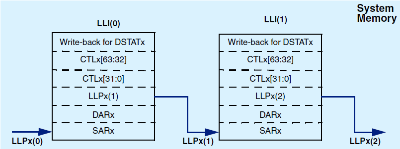
Multi-block transfer using linked lists when DMAC_CHx_STAT_SRC set to false
备注
In order to not confuse the SARx, DARx, LLPx, CTLx, STATx, and DSTATx register locations of the LLI with the corresponding DMAC memory mapped register locations, the LLI register locations are prefixed with LLI; that is, LLI.SARx, LLI.DARx, LLI.LLPx, LLI.CTLx, LLI.SSTATx, and LLI.DSTATx.
The following figures show the mapping of a Linked List Item stored in memory to the channel registers block descriptor.
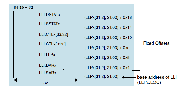
Mapping of block descriptor (LLI) in memory to channel registers when DMAC_CHx_STAT_SRC set to true
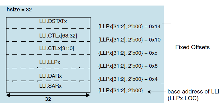
Mapping of block descriptor (LLI) in memory to channel registers when DMAC_CHx_STAT_SRC set to false
Rows 6 through 10 of Programming of transfer types and channel register update method show the required values of LLPx, CTLx, and CFGx for multi-block DMA transfers using block chaining.
备注
For rows 6 through 10 of Programming of transfer types and channel register update method , the LLI.CTLx, LLI.LLPx, LLI.SARx, and LLI.DARx register locations of the LLI are always affected at the start of every block transfer. The LLI.LLPx and LLI.CTLx locations are always used to reprogram the DMAC LLPx and CTLx registers. However, depending on Programming of transfer types and channel register update method row number, the LLI.SARx/LLI.DARx address may or may not be used to reprogram the DMAC SARx/DARx registers.
No. |
Transfer type |
LLP.LOC=0 |
LLP_SRC_EN (CTLx) |
RELOAD_SRC (CRGx) |
LLP_DST_EN (CTLx) |
RELOAD_DST (CRGx) |
CTLx, LLPx update method |
SARx update method |
DARx update method |
Write back |
|---|---|---|---|---|---|---|---|---|---|---|
1 |
Single-block or last transfer of multi-block |
Yes |
0 |
0 |
0 |
0 |
None, user reprograms |
None (Single) |
None (Single) |
No |
2 |
Auto-reload multi-block transfer with contiguous SAR |
Yes |
0 |
0 |
0 |
1 |
CTLx, LLPx are reloaded from initial values |
Contiguous |
Auto-Reload |
No |
3 |
Auto-reload multi-block transfer with contiguous DAR |
Yes |
0 |
1 |
0 |
0 |
CTLx, LLPx are reloaded from initial values |
Auto-Reload |
Contiguous |
No |
4 |
Auto-reload multi-block transfer |
Yes |
0 |
1 |
0 |
1 |
CTLx, LLPx are reloaded from initial values |
Auto-Reload |
Auto-Reload |
No |
5 |
Single-block or last transfer of multi-block |
No |
0 |
0 |
0 |
0 |
None, user reprograms |
None (Single) |
None (Single) |
Yes |
6 |
Linked list multi-block transfer with contiguous SAR |
No |
0 |
0 |
1 |
0 |
CTLx, LLPx loaded from next Linked List item |
Contiguous |
Linked List |
Yes |
7 |
Linked list multi-block transfer with auto-reload SAR |
No |
0 |
1 |
1 |
0 |
CTLx, LLPx loaded from next Linked List item |
Auto-Reload |
Linked List |
Yes |
8 |
Linked list multi-block transfer with contiguous DAR |
No |
1 |
0 |
0 |
0 |
CTLx, LLPx loaded from next Linked List item |
Linked List |
Contiguous |
Yes |
9 |
Linked list multi-block transfer with auto-reload DAR |
No |
1 |
0 |
0 |
1 |
CTLx, LLPx loaded from next Linked List item |
Linked List |
Auto-Reload |
Yes |
10 |
Linked list multi-block transfer |
No |
1 |
0 |
1 |
0 |
CTLx, LLPx loaded from next Linked List item |
Linked List |
Linked List |
Yes |
备注
Throughout this table, there are descriptions about fetching the LLI.CTLx register from the location pointed to by the LLPx register. This exact location is the LLI base address (stored in LLPx register) plus the fixed offset. For example, in Mapping of block descriptor (LLI) in memory to channel registers when DMAC_CHx_STAT_SRC set to true , the location of the LLI.CTLx register is LLPx.LOC + 0xc.
Referring to Programming of transfer types and channel register update method , if the Write Back column entry is “Yes” and the configuration parameter DMAC_CHx_CTL_WB_EN = True, then the CTLx[63:32] register is always written to system memory (to LLI.CTLx[63:32]) at the end of every block transfer. The source status is fetched and written to system memory at the end of every block transfer if the Write Back column entry is “Yes,” DMAC_CHx_CTL_WB_EN = True, DMAC_CHx_STAT_SRC = True, and CFGx.SS_UPD_EN is enabled. The destination status is fetched and written to system memory at the end of every block transfer if the Write Back column entry is “Yes,” DMAC_CHx_CTL_WB_EN = True, DMAC_CHx_STAT_DST = True, and CFGx.DS_UPD_EN is enabled.
The Write back column assumes that the configuration parameter DMAC_CHx_CTL_WB_EN = True. If DMAC_CHx_CTL_WB_EN = False, then there is never writeback of the control and status registers regardless of transfer type, and all rows of this column are “No”.
Auto-Reloading of Channel Registers
During auto-reloading, the channel registers are reloaded with their initial values at the completion of each block and the new values used for the new block. Depending on the row number in Programming of transfer types and channel register update method , some or all of the SARx, DARx, and CTLx channel registers are reloaded from their initial value at the start of a block transfer.
Contiguous Address between Blocks
In this case, the address between successive blocks is selected as a continuation from the end of the previous block.
Enabling the source or destination address to be contiguous between blocks is a function of the CTLx.LLP_SRC_EN, CFGx.RELOAD_SRC, CTLx.LLP_DST_EN, and CTLx.RELOAD_DST registers (see Programming of transfer types and channel register update method ).
备注
You cannot select both SARx and DARx updates to be contiguous. If you want this functionality, you should increase the size of the Block Transfer (CTLx.BLOCK_TS), or if this is at the maximum value, use Row 10 of Programming of transfer types and channel register update method and set up the LLI.SARx address of the block descriptor to be equal to the end SARx address of the previous block. Similarly, set up the LLI.DARx address of the block descriptor to be equal to the end DARx address of the previous block. For more information, refer to “Multi-Block Transfer with Linked List for Source and Linked List for Destination (Row 10)”
Suspension of Transfers between Blocks
At the end of every block transfer, an end-of-block interrupt is asserted if:
Interrupts are enabled, .INT_EN = 1, and
The channel block interrupt is unmasked, MaskBlock[n] = 1, where n is the channel number.
备注
The block-complete interrupt is generated at the completion of the block transfer to the destination.
For rows 6, 8, and 10 of , the DMA transfer does not stall between block transfers. For example, at the end-of-block N, the DMAC automatically proceeds to block (N + 1).
For rows 2, 3, 4, 7, and 9 of Programming of transfer types and channel register update method (SARx and/or DARx auto-reloaded between block transfers), the DMA transfer automatically stalls after the end-of-block interrupt is asserted, if the end-of-block interrupt is enabled and unmasked.
The DMAC does not proceed to the next block transfer until a write to the ClearBlock[n] block interrupt clear register, done by software to clear the channel block-complete interrupt, is detected by hardware.
For rows 2, 3, 4, 7, and 9 of Programming of transfer types and channel register update method (SARx and/or DARx auto-reloaded between block transfers), the DMA transfer does not stall if either:
Interrupts are disabled, CTLx.INT_EN = 0, or
The channel block interrupt is masked, MaskBlock[n] = 0, where n is the channel number.
Channel suspension between blocks is used to ensure that the end-of-block ISR (interrupt service routine) of the next-to-last block is serviced before the start of the final block commences. This ensures that the ISR has cleared the .RELOAD_SRC and/or .RELOAD_DST bits before completion of the final block. The reload bits .RELOAD_SRC and/or .RELOAD_DST should be cleared in the end-of-block ISR for the next-to-last block transfer.
Ending Multi-Block Transfers
All multi-block transfers must end as shown in either Row 1 or Row 5 of Programming of transfer types and channel register update method . At the end of every block transfer, the DMAC samples the row number, and if the DMAC is in the Row 1 or Row 5 state, then the previous block transferred was the last block and the DMA transfer is terminated.
备注
Row 1 and Row 5 are used for single-block transfers or terminating multi-block transfers. Transfers initiated in rows 2, 3 or 4 can only end in row 1; similarly, transfers initiated in rows 6 through 10 can only end in row 5. Ending in the Row 5 state enables status fetch and write-back for the last block. Ending in the Row 1 state disables status fetch and write-back for the last block.
For rows 2, 3, and 4 of Programming of transfer types and channel register update method , (LLPx.LOC = 0 and .RELOAD_SRC and/or .RELOAD_DST is set), multi-block DMA transfers continue until both the .RELOAD_SRC and .RELOAD_DST registers are cleared by software. They should be programmed to 0 in the end-of-block interrupt service routine that services the next-to-last block transfer; this puts the DMAC into the Row 1 state.
For rows 6, 8, and 10 of Programming of transfer types and channel register update method (both .RELOAD_SRC and .RELOAD_DST cleared), the user must set up the last block descriptor in memory so that both LLI.CTLx.LLP_SRC_EN and LLI.CTLx.LLP_DST_EN are 0.
The sampling of the LLPx.LOC bit takes place exclusively at the beginning of the transfer when the channel is enabled. This determines whether writeback is enabled throughout the complete transfer, and changing the value of this bit in subsequent blocks on the same transfer does not have any effect.
备注
The only allowed transitions between the rows of Programming of transfer types and channel register update method are from any row into Row 1 or Row 5. As already stated, a transition into row 1 or row 5 is used to terminate the DMA transfer; all other transitions between rows are not allowed. Software must ensure that illegal transitions between rows do not occur between blocks of a multi-block transfer. For example, if block N is in row 10, then the only allowed rows for block (N +1) are rows 10 or 5.
Disabling a Channel Prior to Transfer Completion
Under normal operation, software enables a channel by writing a 1 to the channel enable register, ChEnReg.CH_EN, and hardware disables a channel on transfer completion by clearing the ChEnReg.CH_EN register bit.
The recommended way for software to disable a channel without losing data is to use the CH_SUSP bit in conjunction with the FIFO_EMPTY bit in the Channel Configuration Register (CFGx).
If software wishes to disable a channel prior to the DMA transfer completion, then it can set the CFGx.CH_SUSP bit to tell the DMAC to halt all transfers from the source peripheral. Therefore, the channel FIFO receives no new data.
Software can now poll the CFGx.FIFO_EMPTY bit until it indicates that the channel FIFO is empty.
The ChEnReg.CH_EN bit can then be cleared by software once the channel FIFO is empty.
When CTLx.SRC_TR_WIDTH < CTLx.DST_TR_WIDTH and the CFGx.CH_SUSP bit is high, the CFGx.FIFO_EMPTY is asserted once the contents of the FIFO do not permit a single word of CTLx.DST_TR_WIDTH to be formed. However, there may still be data in the channel FIFO, but not enough to form a single transfer of CTLx.DST_TR_WIDTH. In this scenario, once the channel is disabled, the remaining data in the channel FIFO is not transferred to the destination peripheral.
It is permissible to remove the channel from the suspension state by writing a 0 to the CFGx.CH_SUSP register. The DMA transfer completes in the normal manner.
备注
If a channel is disabled by software, an active single or burst transaction is not guaranteed to receive an acknowledgement.
If the DMAC is configured to use defined length bursts (DMAC_INCR_BURSTS = 0), disabling the channel via software prior to completing a transfer is not supported.
Abnormal Transfer Termination
A DMAC transfer may be terminated abruptly by software by clearing the channel enable bit, ChEnReg.CH_EN. You must not assume that the channel is disabled immediately after the ChEnReg. The CH_EN bit is cleared over the AHB slave interface. Consider this as a request to disable the channel. You must poll ChEnReg.CH_EN and confirm that the channel is disabled by reading back 0. A case where the channel is not disabled after a channel disable request is where either the source or destination has received a split or retry response. The DMAC must keep re-attempting the transfer to the system HADDR that originally received the split or retry response until an OKAY response is returned; to do otherwise is an AMBA protocol violation.
Software may terminate all channels abruptly by clearing the global enable bit in the DMAC Configuration Register (DmaCfgReg[0]). Again, you must not assume that all channels are disabled immediately after the DmaCfgReg[0] is cleared over the AHB slave interface. Consider this as a request to disable all channels. You must poll ChEnReg and confirm that all channels are disabled by reading back 0.
备注
If the channel enable bit is cleared while there is data in the channel FIFO, this data is not sent to the destination peripheral and is not present when the channel is re-enabled. For read-sensitive source peripherals, such as a source FIFO, this data is therefore lost. When the source is not a read-sensitive device (such as memory), disabling a channel without waiting for the channel FIFO to empty may be acceptable, since the data is available from the source peripheral upon request and is not lost.
If a channel is disabled by software, an active single or burst transaction is not guaranteed to receive an acknowledgement.
If the DMAC is configured to use defined length bursts (DMAC_INCR_BURSTS = 0), disabling the channel via software prior to completing a transfer is not supported.