DSP 内存 Layout
DSP 默认 Layout
DSP 工程是通过 Linker Support Package (LSP) 来描述内存布局。LSP 指定了用于生成可执行文件的目标文件及其内存分布,并为特定目标环境的链接器提供配置便利。
详见《Xtensa Linker Support Packages (LSPs) Reference Manual》(lsp_rm.pdf)。
默认布局示意图如下:

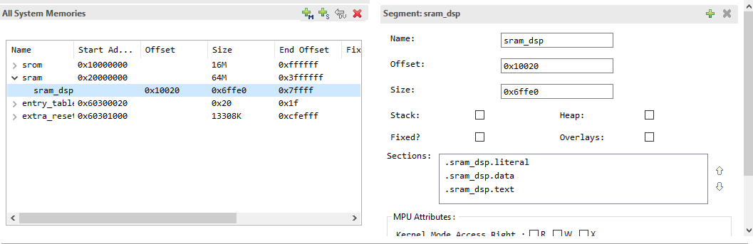
在 Xplorer 中看到的 LSP 示例如下:
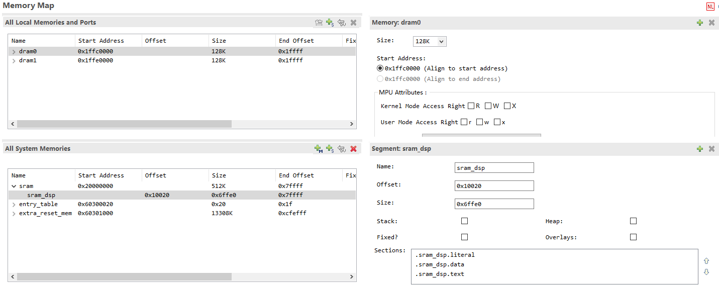
DSP 可使用 sram_dsp、entry_table 和 extra_reset_mem 作为系统内存,DRAM0/1 作为本地数据内存。Reset vector 存放于 entry_table。DRAM0/1 仅能存储数据。
Call0 ABI:可以在 sram_dsp 和 extra_reset_mem 放置代码和数据。
Windowed ABI:代码只能放在 extra_reset_mem,数据可放在 sram_dsp 和 extra_reset_mem。
将代码/数据放到 SRAM
SRAM 的带宽和延迟显著优于 PSRAM。在默认 LSP(RTK_LSP)中包含一个名为 sram_dsp 的段,将代码或数据放入 SRAM 有助于提高计算速度。
使用 C 语言扩展
若需要将单个函数放到 SRAM,可这样声明和定义:
extern void place_into_sram()__attribute__ ((section(".sram_dsp.text")));
void place_into_sram(){
       //detailed implentation
   }
若需要将数据(如数组)放到 SRAM,可这样:
__attribute__ ((section(".sram_dsp.data"))) int array_in_psram[100];
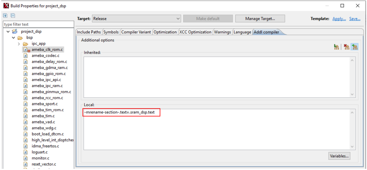
若需要将某个源文件(如
ameba_clk_rom.c)的所有函数都放到 SRAM:右键该文件,选择
Build Properties,在弹窗中将相关选项设置为 No 。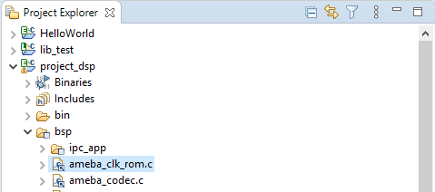
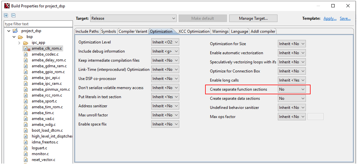
然后切换到 Addl compiler 选项卡,添加自定义编译参数,如下图:
更改 LSP 的默认 Layout
MCU 与 DSP 共享 PSRAM 和 SRAM,但 DTCM 仅供 DSP 使用。当 MCU 的 PSRAM Layout 发生变化时,需同步修改 DSP 的 LSP。 通常 DTCM 和 SRAM 地址保持默认,仅调整 PSRAM 的起止地址。PSRAM 的地址调整方法如下:
进入目录
{SDK}/project/img_utilitycd {SDK}/project/img_utility
运行
python lsp_modify.py可查看当前 DSP PSRAM 地址:>> python lsp_modify.py Current LSP psram: Start Address: 0x60300000, End Address: 0x61000000, Size: 0xd00000 Invalid input. Please enter the start and end addresses in hex. Example: "python lsp_modify.py 0x60300000 0x61000000" DSP link script change FAIL.
运行
python lsp_modify.py <start psram address in hex> <end psram address in hex>可直接生成新的 LSP 并输出新的 LSP 信息:>> python lsp_modify.py 0x60400000 0x60A00000 Current LSP psram: Start Address: 0x60300000, End Address: 0x61000000, Size: 0xd00000 New LSP psram: Start Address: 0x60400000, End Address: 0x60a00000, Size: 0x600000 Warning : 'entry_table' start address not aligned to MPU min alignment (is 0x60400020, min alignment is 0x00001000) Warning : MPU region size smaller than min region size (0x60400020 - 0x60400040, is 32 must be at least 4096 bytes) Warning : 'unused' start address not aligned to MPU min alignment (is 0x60400040, min alignment is 0x00001000) New linker scripts generated in ../../project/RTK_LSP/RI-2021.8/HIFI5_PROD_1123_asic_UPG/RTK_LSP/ldscripts Change MCU layout (amebalite_layout.ld) PSRAM_DSP_START to 0x60400000
本例将 PSRAM 起止地址调整为 0x60400000/0x60A00000,因脚本会自动生成 MPU table,上述的地址对齐警告可忽略,无实际影响。
在 link 脚本
RTK_LSP/ldscripts/elf32xtensa.x中增加 KEEP 关键字:.ipc_table : ALIGN(4) { _ipc_table_start = ABSOLUTE(.); KEEP(*(.ipc_table)) . = ALIGN (4); _ipc_table_end = ABSOLUTE(.); } >psram0_seg :psram0_phdr .command : ALIGN(4) { _command_start = ABSOLUTE(.); KEEP(*(.command)) . = ALIGN (4); _command_end = ABSOLUTE(.); } >psram0_seg :psram0_phdr
根据上述脚本输出修改 MCU 的内存布局文件(
{MCU_SDK}/amebalite_gcc_project/amebalite_layout.ld):#define PSRAM_DSP_START (0x60400000)重新编译 DSP 与 MCU 工程。
备注
使用脚本前,需确保 Xtensa 工具链的 bin 目录已加入系统/用户 PATH,否则找不到可执行文件。
若曾修改过 MPU 其它属性,请在新生成的
mpu_table.c上同步修改。确保新生成的
mpu_table.c已加入编译工程。