Cache
Introduction
The following table lists the cache attribution of the chip.
Processor |
Type |
Size (bytes) |
Way |
|---|---|---|---|
KM4TZ |
I-Cache |
16K |
4 |
D-Cache |
16K |
4 |
|
KM4NS |
I-Cache |
16K |
4 |
D-Cache |
16K |
4 |
KM0 Cache
The cache operation of KM0 is similar to that of KM4, but the cache registers of KM0 are not banked between Security States. Refer to Arm®v8-M Architecture Reference Manual for cache memories characteristics.
KM4 Cache
The KM4 processor can cache data and instructions that meet certain memory attribute criteria.
L1 Instruction Cache
is virtually indexed and physically tagged.
is 4-way set associative.
is configurable to 16KB.
uses a cache line length of 32 bytes.
uses a pseudo-random replacement policy.
Dynamic program flow prediction.
L1 Data Cache
is physically indexed and physically tagged.
is 4-way set associative.
is configurable to 16KB.
uses a cache line length of 32 bytes.
uses a pseudo-random replacement policy.
KM4 Cache Way Restricted
The KM4 cache adds a new function of way restricting.
We can define a restricted address range. The data in the restricted address range is stored in specified ways. The data out of the restricted address range would be stored in other ways.
The address range can be defined using the following registers:
ICWRR_BASE~ICWRR_TOP: define the restricted address range which stored in specified I-Cache ways.
DCWRR_BASE~DCWRR_TOP: define the restricted address range which stored in specified D-Cache ways.
The specified I-Cache ways can be configured using ACTLR.ICWRR_MODE[1:0].
ACTLR.ICWRR_MODE[1:0] |
Data in restricted range |
Data not in restricted range |
|---|---|---|
2’b00 |
Uses way 0 |
Uses way 1, way 2, and way 3 |
2’b01 |
Uses way 0 and way 1 |
Uses way 2 and way 3 |
2’b10 |
Uses way 0, way 1, and way 2 |
Uses way 3 |
2’b11 |
Uses all ways |
Uses no ways |
The specified D-Cache ways can be configured using ACTLR.DCWRR_MODE[1:0].
ACTLR.DCWRR_MODE[1:0] |
Data in restricted range |
Data not in restricted range |
|---|---|---|
2’b00 |
Uses way 0 |
Uses way 1, way 2, and way 3 |
2’b01 |
Uses way 0 and way 1 |
Uses way 2 and way 3 |
2’b10 |
Uses way 0, way 1, and way2 |
Uses way 3 |
2’b11 |
Uses all ways |
Uses no ways |
The following figure shows the case of restricting D-Cache ways for a specified address range. In this case, ACTLR.DCWRR_MODE[1:0] is set to 2’b00, which means using way 0. The data in the restricted address range would be stored in way 0, and the data out of the restricted address range would be stored in way 1 to way 3. In this way, way 0 is occupied by the restricted address range independently. The data in this way would not be evicted by the data out of the restricted address range.
If there is some efficiency-critical code or data, this function would help to reserve several ways for it.

Restricting D-Cache ways for a specified address range
This function would also be used to reserve several ways for TCM, which is introduced in the next section.
KM4 Cache and TCM
In section 2.4.1, we introduce that the specified cache ways can be configured to be used by a restricted address range, and the other ways to be used by other address. If we set the restricted address range to the whole address space, other ways would not be used by cache. Users can configure the left ways as TCM (Tightly-Coupled Memory).

KM4 Cache and TCM
The TCM is a zero-wait-state memory, which would be allocated an address, while the cache has no address. That is the difference between TCM and cache and why the TCM can be used to store specified program and efficiency-critical code or data, such as interrupt service routines. Unlike the Cache, the code or data in the TCM would not be replaced out.
The total memory size of the KM4 cache SRAM is 96KB, in which I-Cache is 64KB and D-Cache is 32KB. Several software-configurable options differ in the size of cache, the size of TCM, and the cache associativity. Users can select the option which maximizes the performance by setting cache way restricted registers.
The cache system features configurable 1/2/3/4-way set associative. It can be configured to the following combinations:
96KB TCM, no cache
80KB TCM, 0KB D-Cache, 16KB I-Cache
64KB TCM, 16KB D-Cache, 16KB I-Cache
48KB TCM, 16KB D-Cache, 32KB I-Cache
32KB TCM, 16KB D-Cache, 48KB I-Cache
16KB TCM, 32KB D-Cache, 48KB I-Cache
0KB TCM, 32KB D-Cache, 64KB I-Cache
These different configurations provide flexibility for software to adjust and reach optimum system performance.

KM4 cache and TCM configuration
The address mapping of these memories is shown below.
ACTLR.ICWRR_MODE[1:0] |
ACTLR.DCWRR_MODE[1:0] |
Memory distribution |
Memory distribution |
Memory distribution |
|---|---|---|---|---|
ACTLR.ICWRR_MODE[1:0] |
ACTLR.DCWRR_MODE[1:0] |
Cache |
Used as TCM, address mapping |
TCM Size |
2’b11 |
2’b11 |
I-Cache 64KB, 4 way (way 0/1/2/3) |
0KB |
|
2’b11 |
2’b11 |
D-Cache 32KB, 4 way (way 0/1/2/3) |
0KB |
|
2’b10 |
2’b11 |
I-Cache 48KB, 3 way (way 0/1/2) |
TCM0_ICache: 0x0008_0000 ~ 0x0008_3FFF (way 3) |
16KB |
2’b10 |
2’b11 |
D-Cache 32KB, 4 way (way 0/1/2/3) |
16KB |
|
2’b10 |
2’b01 |
I-Cache 48KB, 3 way (way 0/1/2) |
TCM0_ICache: 0x0008_0000 ~ 0x0008_3FFF (way 3) |
32KB |
2’b10 |
2’b01 |
D-Cache 16KB, 2 way (way 0/1) |
TCM0_DCache: 0x0008_4000 ~ 0x0008_5FFF (way 3) TCM0_DCache: 0x0008_6000 ~ 0x0008_7FFF (way 2) |
32KB |
2’b01 |
2’b01 |
I-Cache 32KB, 2 way (way 0/1) |
TCM0_ICache: 0x0008_0000 ~ 0x0008_3FFF (way 3) TCM1_ICache: 0x0008_8000 ~ 0x0008_BFFF (way 2) |
48KB |
2’b01 |
2’b01 |
D-Cache 16KB, 2 way (way 0/1) |
TCM0_DCache: 0x0008_4000 ~ 0x0008_5FFF (way 3) TCM0_DCache: 0x0008_6000 ~ 0x0008_7FFF (way 2) |
48KB |
2’b00 |
2’b01 |
I-Cache 16KB, 1 way (way 0) |
TCM0_ICache: 0x0008_0000 ~ 0x0008_3FFF (way 3) TCM1_ICache: 0x0008_8000 ~ 0x0008_BFFF (way 2) TCM2_ICache: 0x0008_C000 ~ 0x0008_FFFF (way 1) |
64KB |
2’b00 |
2’b01 |
D-Cache 16KB, 2 way (way 0/1) |
TCM0_DCache: 0x0008_4000 ~ 0x0008_5FFF (way 3) TCM0_DCache: 0x0008_6000 ~ 0x0008_7FFF (way 2) |
64KB |
2’b00 |
Cache disable |
I-Cache 16KB, 1 way (way 0) |
TCM0_ICache: 0x0008_0000 ~ 0x0008_3FFF (way 3) TCM1_ICache: 0x0008_8000 ~ 0x0008_BFFF (way 2) TCM2_ICache: 0x0008_C000 ~ 0x0008_FFFF (way 1) |
80KB |
2’b00 |
Cache disable |
D-Cache disable |
TCM0_DCache: 0x0008_4000 ~ 0x0008_5FFF (way 3) TCM0_DCache: 0x0008_6000 ~ 0x0008_7FFF (way 2) TCM0_DCache: 0x0009_0000 ~ 0x0009_1FFF (way 1) TCM0_DCache: 0x0009_2000 ~ 0x0009_3FFF (way 0) |
80KB |
Cache disable |
Cache disable |
No cache |
TCM0_ICache: 0x0008_0000 ~ 0x0008_3FFF (way 3) TCM1_ICache: 0x0008_8000 ~ 0x0008_BFFF (way 2) TCM2_ICache: 0x0008_C000 ~ 0x0008_FFFF (way 1) TCM2_ICache: 0x0009_4000 ~ 0x0009_7FFF (way 0) |
96KB |
Cache disable |
Cache disable |
No cache |
TCM0_DCache: 0x0008_4000 ~ 0x0008_5FFF (way 3) TCM0_DCache: 0x0008_6000 ~ 0x0008_7FFF (way 2) TCM0_DCache: 0x0009_0000 ~ 0x0009_1FFF (way 1) TCM0_DCache: 0x0009_2000 ~ 0x0009_3FFF (way 0) |
96KB |
Before setting way restricted mode registers, the cache way restricted range should be set to the total address mapping (from 0x0000_0000 to 0xFFFF_0000 defined by ICWRR_TOP or DCWRR_TOP) to avoid cache accessing in TCM memory. For the continuity of TCM address, I-Cache and D-Cache way restricted mode should be the same.
Registers
The following table provides the memory map of KM4 cache registers. All registers are addressed at 32-bit boundary. Where the physical size of any register is less than 32-bit wide, the upper unused bits of the 32-bit boundary are reserved. Writing to these bits has no effect; reading from these bits returns 0.
Name |
Address offset |
Description |
|---|---|---|
SCB_CLIDR |
0xE000_ED78 |
Cache Level ID register |
SCB_CTR |
0xE000_ED7C |
Cache Type register |
SCB_CCSIDR |
0xE000_ED80 |
Cache Size ID Register |
SCB_CSSELR |
0xE000_ED84 |
Cache Size Selection Register |
SCB_ICIALLU |
0xE000_EF50 |
I-Cache Invalidation All to PoU |
SCB_ICIMVAU |
0xE000_EF58 |
I-Cache Invalidation by MVA to PoU |
SCB_DCIMVAC |
0xE000_EF5C |
D-Cache Invalidation by MVA to PoC |
SCB_DCISW |
0xE000_EF60 |
D-Cache Invalidation by Set-way |
SCB_DCCMVAU |
0xE000_EF64 |
D-Cache Cleaning by MVA to PoU |
SCB_DCCMVAC |
0xE000_EF68 |
D-Cache Cleaning by MVA to PoC |
SCB_DCCSW |
0xE000_EF6C |
D-Cache Cleaning by Set-way |
SCB_DCCIMVAC |
0xE000_EF70 |
D-Cache Cleaning and Invalidation by MVA to PoC |
SCB_DCCISW |
0xE000_EF74 |
D-Cache Cleaning and Invalidation by Set-way |
ACTLR |
0xE000_E008 |
Auxiliary Control Register |
ICWRR_BASE |
0xE004_20A0 |
I-Cache Way Restricted Range Base Address Register |
ICWRR_TOP |
0xE004_20A4 |
I-Cache Way Restricted Range Top Address Register |
DCWRR_BASE |
0xE004_20A8 |
D-Cache Way Restricted Range Base Address Register |
DCWRR_TOP |
0xE004_20AC |
D-Cache Way Restricted Range Top Address Register |
DTCM0_BASE |
0xE004_2060 |
DTCM0 Base Address |
DTCM0_TOP |
0xE004_2064 |
DTCM0 Top Address |
SCB_CLIDR
The SCB_CLIDR characteristics are:
Purpose: Identifies the type of caches implemented and the level of coherency and unification.
Usage constraints:
Privileged access permitted only. Unprivileged accesses generate a fault.
This register is word accessible only. Half-word and byte accesses are UNPREDICTABLE.
From Armv8.1-M, this register is accessible to accesses through unprivileged DAP requests when either DAUTHCTRL_S.UIDAPEN or DAUTHCTRL_NS.UIDAPEN is set.
Configurations: This register is always implemented.
Attributes:
32-bit read-only register located at 0xE000_ED78.
Secure software can access the Non-secure version of this register via CLIDR_NS located at 0xE002_ED78.
The location 0xE002_ED78 is RES0 to software executing in Non-secure state and the debugger.
This register is not banked between Security states.
Default value: 0x4920_0003
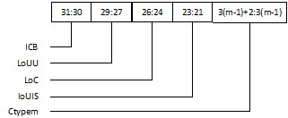
Bit |
Symbol |
Access |
Description |
|---|---|---|---|
31:30 |
ICB |
RO |
Inner cache boundary. This field indicates the boundary between inner and outer domain. The possible values of this field are:
|
29:27 |
LoUU |
RO |
Level of Unification Uniprocessor. This field indicates the Level of Unification Uniprocessor for the cache hierarchy. |
26:24 |
LoC |
RO |
Level of Coherence. This field indicates the Level of Coherence for the cache hierarchy. |
23:21 |
LoUIS |
RO |
Level of Unification Inner Shareable. This field indicates the Level of Unification Shareable for the cache hierarchy. |
3(m-1)+2:3(m-1) (m = 1 to 7) |
Ctypem |
RO |
Cache type field m. Indicates the type of cache implemented at level m. The possible values of this field are:
All other values are reserved. |
SCB_CTR
The SCB_CTR characteristics are:
Purpose: Provides information about the architecture of the caches.
Usage constraints:
Privileged access permitted only. Unprivileged accesses generate a fault.
This register is word accessible only. Half-word and byte accesses are UNPREDICTABLE.
From Armv8.1-M, this register is accessible to accesses through unprivileged DAP requests when either DAUTHCTRL_S.UIDAPEN or DAUTHCTRL_NS.UIDAPEN is set.
Configurations: This register is always implemented.
Attributes:
32-bit read-only register located at 0xE000_ED7C.
Secure software can access the Non-secure version of this register via CTR_NS located at 0xE002_ED7C.
The location 0xE002_ED7C is RES0 to software executing in Non-secure state and the debugger.
This register is banked between Security states.
Default value: 0x8303_C003
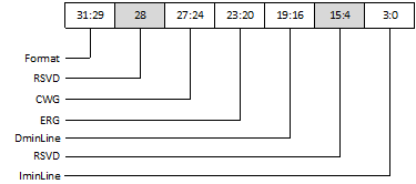
Bit |
Symbol |
Access |
Description |
|---|---|---|---|
31:29 |
Format |
RO |
Cache Type Register format. Indicates whether cache type information is provided. The possible values of this field are:
|
28 |
RSVD |
Reserved |
|
27:24 |
CWG |
RO |
Cache Write-Back Granule. Log2 of the number of words of the maximum size of memory that can be overwritten as a result of the eviction of a cache entry that has had a memory location in it modified. The possible values of this field are:
|
23:20 |
ERG |
RO |
Exclusives Reservation Granule. Log2 of the number of words of the maximum size of the reservation granule that has been implemented for the Load-Exclusive and Store-Exclusive instructions. The possible values of this field are:
|
19:16 |
DminLine |
RO |
Data cache minimum line length. Log2 of the number of words(4 bytes) in the smallest cache line of all the data caches and unified caches that are controlled by the PE. |
15:4 |
RSVD |
Reserved |
|
3:0 |
IminLine |
RO |
Instruction cache minimum line length. Log2 of the number of words in the smallest cache line of all the instruction caches that are controlled by the PE. |
SCB_CCSIDR
The CCSIDR characteristics are:
Purpose: The CCSIDR provides information about the architecture of the currently selected cache.
Usage constraints:
Privileged access permitted only. Unprivileged accesses generate a fault.
This register is word accessible only. Half-word and byte accesses are UNPREDICTABLE.
From Armv8.1-M, this register is accessible to accesses through unprivileged DAP requests when either DAUTHCTRL_S.UIDAPEN or DAUTHCTRL_NS.UIDAPEN is set.
If CSSELR points to an unimplemented cache, the value of this register is UNKNOWN.
Configurations: This register is always implemented.
Attributes:
32-bit read-only register located at 0xE000_ED80.
Secure software can access the Non-secure version of this register via CCSIDR_NS located at 0xE002_ED80.
The location 0xE002_ED80 is RES0 to software executing in Non-secure state and the debugger.
This register is banked between Security states.
Preface:
Provides indirect read access to the architecture of the cache currently selected by CSSELR. The parameters NumSets, Associativity, and LineSize in these registers define the architecturally visible parameters that are required for the cache maintenance by Set/Way instructions. They are not guaranteed to represent the actual microarchitectural features of a design. You cannot make any inference about the actual sizes of caches based on these parameters.
Default value:
KM0: D-Cache 0xF00F_E009, I-Cache 0xE01F_E009
KM4: D-Cache 0xF01F_E019, I-Cache 0xE03F_E019
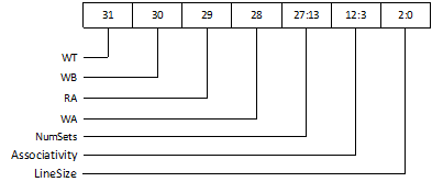
Bit |
Symbol |
Access |
Description |
|---|---|---|---|
31 |
WT |
RO |
Write-Through. Indicates whether the currently selected cache level supports Write-Through. The possible values of this bit are:
|
30 |
WB |
RO |
Write-Back. Indicates whether the currently selected cache level supports Write-Back. The possible values of this bit are:
|
29 |
RA |
RO |
Read-Allocation. Indicates whether the currently selected cache level supports Read-Allocation. The possible values of this bit are:
|
28 |
WA |
RO |
Write-Allocation. Indicates whether the currently selected cache level supports Write-Allocation. The possible values of this bit are:
|
27:13 |
NumSets |
RO |
Number of sets. Indicates (number of sets in the currently selected cache) - 1. Therefore, a value of 0 indicates that 1 set in the cache. The number of sets does not have to be a power of 2. |
12:3 |
Associativity |
RO |
Associativity. Indicates (the associativity of cache) - 1. A value of 0 indicates an associativity of 1. The associativity does not have to be a power of 2. |
2:0 |
LineSize |
RO |
Line size. Indicates (log2(number of words per line in the currently selected cache)) - 2. |
SCB_CSSELR
The SCB_CSSELR characteristics are:
Purpose: Selects the current Cache Size ID Register, CCSIDR, by specifying the required cache level and the cache type (either instruction or data cache)
Usage constraints:
Privileged access permitted only. Unprivileged accesses generate a fault.
This register is word accessible only. Half-word and byte accesses are UNPREDICTABLE.
From Armv8.1-M, this register is accessible to accesses through unprivileged DAP requests when either DAUTHCTRL_S.UIDAPEN or DAUTHCTRL_NS.UIDAPEN is set.
Configurations: This register is always implemented.
Attributes:
32-bit read/write register located at 0xE000_ED84.
Secure software can access the Non-secure version of this register via CSSELR_NS located at 0xE002_ED84.
The location 0xE002_ED84 is RES0 to software executing in Non-secure state and the debugger.
This register is banked between Security states.
From Armv8.1-M onwards it is IMPLEMENTATION DEFINED whether a debugger write to this register is ignored when the PE is not in Debug state.
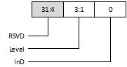
Bit |
Symbol |
Access |
Description |
|---|---|---|---|
31:4 |
RSVD |
Reserved |
|
3:1 |
Level |
R/W |
Cache level. Selects which cache level is to be identified. Permitted values are from 0b000, indicating Level 1 cache, to 0b110 indicating Level 7 cache. The possible values of this field are:
|
0 |
InD |
R/W |
Instruction not data. Selects whether the instruction or the data cache is to be identified. The possible values of this bit are:
|
SCB_ICIALLU
The SCB_ICIALLU characteristics are:
Purpose: Invalidate all instruction caches to PoU.
Usage constraints:
Privileged access permitted only. Unprivileged accesses generate a fault.
This register is word accessible only. Half-word and byte accesses are UNPREDICTABLE.
From Armv8.1-M, this register is accessible to accesses through unprivileged DAP requests when either DAUTHCTRL_S.UIDAPEN or DAUTHCTRL_NS.UIDAPEN is set.
Configurations: This register is always implemented.
Attributes:
32-bit write-only register located at 0xE000_EF50.
Secure software can access the Non-secure version of this register via ICIALLU_NS located at 0xE002_EF50.
The location 0xE002_EF50 is RES0 to software executing in Non-secure state and the debugger.
This register is not banked between Security states.
Bit |
Symbol |
Access |
Description |
|---|---|---|---|
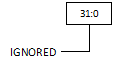
31:0 |
IGNORED |
WO |
The value written to this field is ignored. Ignored. |
SCB_ICIMVAU
The SCB_ICIMVAU characteristics are:
Purpose: Invalidate instruction cache line by address to PoU.
Usage constraints:
Privileged access permitted only. Unprivileged accesses generate a fault.
This register is word accessible only. Half-word and byte accesses are UNPREDICTABLE.
From Armv8.1-M, this register is accessible to accesses through unprivileged DAP requests when either DAUTHCTRL_S.UIDAPEN or DAUTHCTRL_NS.UIDAPEN is set.
Configurations: This register is always implemented.
Attributes:
32-bit write-only register located at 0xE000EF58.
Secure software can access the Non-secure version of this register via ICIMVAU_NS located at 0xE002_EF58. The location 0xE002_EF58 is RES0 to software executing in Non-secure state and the debugger.
This register is not banked between Security states.

Bit |
Symbol |
Access |
Description |
|---|---|---|---|
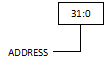
31:0 |
ADDRESS |
WO |
Address. Writing to this field initiates the maintenance operation for the address written. |
SCB_DCIMVAC
The DCIMVAC characteristics are:
Purpose: Invalidate data or unified cache line by address to PoC.
Usage constraints:
Privileged access permitted only. Unprivileged accesses generate a fault.
This register is word accessible only. Half-word and byte accesses are UNPREDICTABLE.
Configurations: This register is always implemented.
Attributes:
32-bit write-only register located at 0xE000_EF5C.
Secure software can access the Non-secure version of this register via DCIMVAC_NS located at 0xE002_EF5C. The location 0xE002_EF5C is RES0 to software executing in Non-secure state and the debugger.
This register is not banked between Security states.

Bit |
Symbol |
Access |
Description |
|---|---|---|---|
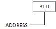
31:0 |
ADDRESS |
WO |
Address. Writing to this field initiates the maintenance operation for the address written. |
SCB_DCISW
The SCB_DCISW characteristics are:
Purpose: Invalidate data or unified cache line by set/way.
Usage constraints:
Privileged access permitted only. Unprivileged accesses generate a fault.
This register is word accessible only. Half-word and byte accesses are UNPREDICTABLE.
Configurations: This register is always implemented.
Attributes:
32-bit write-only register located at 0xE000_EF60.
Secure software can access the Non-secure version of this register via DCISW_NS located at 0xE002_EF60.
The location 0xE002_EF60 is RES0 to software executing in Non-secure state and the debugger.
This register is not banked between Security states.
Bit |
Symbol |
Access |
Description |
|---|---|---|---|
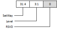
31:4 |
SetWay |
WO |
Cache set/way. Contains two fields:
Bits[L-1:4] are RES0. A = Log2(ASSOCIATIVITY), L = Log2(LINELEN), B = (L + S), S = Log2(NSETS). ASSOCIATIVITY, LINELEN (line length, in bytes), and NSETS (number of sets) have their usual meanings and are the values for the cache level being operated on. The values of A and S are rounded up to the next integer. |
3:1 |
Level |
WO |
Cache level. Cache level to operate on, minus 1. For example, this field is 0 for operations on L1 cache, or 1 for operations on L2 cache. |
0 |
RSVD |
Reserved |
SCB_DCCMVAU
The SCB_DCCMVAU characteristics are:
Purpose: Clean data or unified cache line by address to PoU.
Usage constraints:
Privileged access permitted only. Unprivileged accesses generate a fault.
This register is word accessible only. Half-word and byte accesses are UNPREDICTABLE.
From Armv8.1-M, this register is accessible to accesses through unprivileged DAP requests when either DAUTHCTRL_S.UIDAPEN or DAUTHCTRL_NS.UIDAPEN is set.
Configurations: This register is always implemented.
Attributes:
32-bit write-only register located at 0xE000_EF64.
Secure software can access the Non-secure version of this register via DCCMVAU_NS located at 0xE002_EF64. The location 0xE002_EF64 is RES0 to software executing in Non-secure state and the debugger.
This register is not banked between Security states.
Bit |
Symbol |
Access |
Description |
|---|---|---|---|
31:0 |
ADDRESS |
WO |
Address. Writing to this field initiates the maintenance operation for the address written. |
SCB_DCCMVAC
The SCB_DCCMVAC characteristics are:
Purpose: Clean data or unified cache line by address to PoC.
Usage constraints:
Privileged access permitted only. Unprivileged accesses generate a fault.
This register is word accessible only. Half-word and byte accesses are UNPREDICTABLE.
From Armv8.1-M, this register is accessible to accesses through unprivileged DAP requests when either DAUTHCTRL_S.UIDAPEN or DAUTHCTRL_NS.UIDAPEN is set.
Configurations: This register is always implemented.
Attributes:
32-bit write-only register located at 0xE000_EF68.
Secure software can access the Non-secure version of this register via DCCMVAC_NS located at 0xE002_EF68. The location 0xE002_EF68 is RES0 to software executing in Non-secure state and the debugger.
This register is not banked between Security states.

Bit |
Symbol |
Access |
Description |
|---|---|---|---|
31:0 |
ADDRESS |
WO |
Address. Writing to this field initiates the maintenance operation for the address written. |
SCB_DCCSW
The SCB_DCCSW characteristics are:
Purpose: Clean data or unified cache line by set/way.
Usage constraints:
Privileged access permitted only. Unprivileged accesses generate a fault.
This register is word accessible only. Half-word and byte accesses are UNPREDICTABLE.
From Armv8.1-M, this register is accessible to accesses through unprivileged DAP requests when either DAUTHCTRL_S.UIDAPEN or DAUTHCTRL_NS.UIDAPEN is set.
Configurations: This register is always implemented.
Attributes:
32-bit write-only register located at 0xE000_EF6C.
Secure software can access the Non-secure version of this register via DCCSW_NS located at 0xE002_EF6C.
The location 0xE002_EF6C is RES0 to software executing in Non-secure state and the debugger.
This register is not banked between Security states.

Bit |
Symbol |
Access |
Description |
|---|---|---|---|
31:4 |
SetWay |
WO |
Cache set/way. Contains two fields:
Bits [L-1:4] are RES0. A = Log2(ASSOCIATIVITY), L = Log2(LINELEN), B = (L + S), S = Log2(NSETS). ASSOCIATIVITY, LINELEN (line length, in bytes), and NSETS (number of sets) have their usual meanings and are the values for the cache level being operated on. The values of A and S are rounded up to the next integer. |
3:1 |
Level |
WO |
Cache level. Cache level to operate on, minus 1. For example, this field is 0 for operations on L1 cache, or 1 for operations on L2 cache. |
0 |
RSVD |
Reserved |
SCB_DCCIMVAC
The SCB_DCCIMVAC characteristics are:
Purpose: Clean and invalidate data or unified cache line by address to PoC.
Usage constraints:
Privileged access permitted only. Unprivileged accesses generate a fault.
This register is word accessible only. Half-word and byte accesses are UNPREDICTABLE.
From Armv8.1-M, this register is accessible to accesses through unprivileged DAP requests when either DAUTHCTRL_S.UIDAPEN or DAUTHCTRL_NS.UIDAPEN is set.
Configurations: This register is always implemented.
Attributes:
32-bit write-only register located at 0xE000_EF70.
Secure software can access the Non-secure version of this register via DCCIMVAC_NS located at 0xE002_EF70. The location 0xE002_EF70 is RES0 to software executing in Non-secure state and the debugger.
This register is not banked between Security states.
Bit |
Symbol |
Access |
Description |
|---|---|---|---|
31:0 |
ADDRESS |
WO |
Address. Writing to this field initiates the maintenance operation for the address written. |
SCB_DCCISW
The SCB_DCCISW characteristics are:
Purpose: Clean and invalidate data or unified cache line by set/way.
Usage constraints:
Privileged access permitted only. Unprivileged accesses generate a fault.
This register is word accessible only. Half-word and byte accesses are UNPREDICTABLE.
From Armv8.1-M, this register is accessible to accesses through unprivileged DAP requests when either DAUTHCTRL_S.UIDAPEN or DAUTHCTRL_NS.UIDAPEN is set.
Configurations: This register is always implemented.
Attributes:
32-bit write-only register located at 0xE000_EF74.
Secure software can access the Non-secure version of this register via DCCISW_NS located at 0xE002_EF74.
The location 0xE002_EF74 is RES0 to software executing in Non-secure state and the debugger.
This register is not banked between Security states.

Bit |
Symbol |
Access |
Description |
|---|---|---|---|
31:4 |
SetWay |
WO |
Cache set/way. Contains two fields:
Bits [L-1:4] are RES0. A = Log2(ASSOCIATIVITY), L = Log2(LINELEN), B = (L + S), S = Log2(NSETS). ASSOCIATIVITY, LINELEN (line length, in bytes), and NSETS (number of sets) have their usual meanings and are the values for the cache level being operated on. The values of A and S are rounded up to the next integer. |
3:1 |
Level |
WO |
Cache level. Cache level to operate on, minus 1. For example, this field is 0 for operations on L1 cache, or 1 for operations on L2 cache. |
0 |
RSVD |
Reserved |
ACTLR
The ACTLR characteristics are:
Purpose: Provides IMPLEMENTATION DEFINED configuration and control options.
Usage constraints:
Privileged access permitted only. Unprivileged accesses generate a fault.
This register is word accessible only. Half-word and byte accesses are UNPREDICTABLE.
Configurations: This register is always implemented.
Attributes:
32-bit read/write register located at 0xE000_E008.
Secure software can access the Non-secure version of this register via ACTLR_NS located at 0xE002_E008.
The location 0xE002_E008 is RES0 to software executing in Non-secure state and the debugger.
It is IMPLEMENTATION DEFINED whether this register is banked between Security states.
From Armv8.1-M onwards it is IMPLEMENTATION DEFINED whether a debugger write to this register is ignored when the PE is not in Debug state.
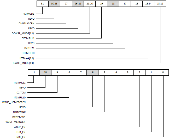
Bit |
Symbol |
Access |
Description |
||||||||||||||||||||||||
|---|---|---|---|---|---|---|---|---|---|---|---|---|---|---|---|---|---|---|---|---|---|---|---|---|---|---|---|
31 |
RETMODE |
RO |
Indicates the core is reset from retention mode or not.
Reset value is controlled by the input pin in retention mode. |
||||||||||||||||||||||||
30:28 |
RSVD |
Reserved |
|||||||||||||||||||||||||
27 |
DMASLACCEN |
R/W |
DMA in sleep enable.
Reset value is 0. RAZ/WI if EXT_DMA==NO |
||||||||||||||||||||||||
26:22 |
RSVD |
Reserved |
|||||||||||||||||||||||||
21:20 |
DCWRR_MODE[1:0] |
R/W |
Data Cache Way Restricted Operation Mode When data cache is 4-way associated:
When data cache is 2-way associated:
Reset value is 2’b11. RAZ/WI if DCACHE==NONE |
||||||||||||||||||||||||
19 |
DTCMFILL1 |
WO |
Writing 1 to this bit triggers the core to fill its DTCM1. Writing 0 has no effect. |
||||||||||||||||||||||||
18 |
RSVD |
Reserved |
|||||||||||||||||||||||||
17 |
D2DTCM |
R/W |
Instruction fetch from DTCM enable. The reset value is derived from INITD2DTCM pin. |
||||||||||||||||||||||||
16 |
DTCMFILL0 |
WO |
Writing 1 to this bit triggers the core to fill its DTCM. Writing 0 has no effect. |
||||||||||||||||||||||||
15:14 |
IPFMask[1:0] |
R/W |
ISide prefetch number.
|
||||||||||||||||||||||||
13:12 |
ICWRR_MODE[1:0] |
R/W |
Instruction Cache Way Restricted Operation Mode When instruction cache is 4-way associated:
When instruction cache is 2-way associated:
Reset value is 2’b11. RAZ/WI if ICACHE==NONE |
||||||||||||||||||||||||
11 |
ITCMFILL1 |
WO |
Writing 1 to this bit triggers the core to fill its ITCM1. Writing 0 has no effect. |
||||||||||||||||||||||||
10 |
RSVD |
Reserved |
|||||||||||||||||||||||||
9 |
D2ITCM |
R/W |
Data load store to and from ITCM enable. The reset value is derived from INITD2ITCM pin. |
||||||||||||||||||||||||
8 |
ITCMFILL0 |
WO |
Writing 1 to this bit triggers the core to fill its ITCM. Writing 0 has no effect. |
||||||||||||||||||||||||
7 |
WBUF_UCMERGEEN |
R/W |
Write buffer merge enable for uncacheable requests
Reset value is 0. |
||||||||||||||||||||||||
6 |
RSVD |
Reserved |
|||||||||||||||||||||||||
5 |
D2ITCMNC |
R/W |
Data load store request hits ITCM is forced to be non-cacheable.
Reset value is 0. |
||||||||||||||||||||||||
4 |
D2ITCMWB |
R/W |
Data load store request hits ITCM is forced to be write-back.
Reset value is 0. |
||||||||||||||||||||||||
3 |
WBUF_MERGEEN |
R/W |
Write buffer merge enable.
Reset value is 1. |
||||||||||||||||||||||||
2 |
WBUF_EN |
R/W |
Write buffer enable.
Reset value is 1. |
||||||||||||||||||||||||
1 |
LUB_EN |
R/W |
Load-use date buffer enable.
Reset value is 1. |
||||||||||||||||||||||||
0 |
NBL_EN |
R/W |
Non-blocking load enable.
Reset value is 1. |
ICWRR_BASE
The ICWRR_BASE characteristics are:
Purpose: Provides Instruction Cache Way Restricted Range base.
Usage constraints:
Privileged access permitted only. Unprivileged accesses generate a fault.
This register is word accessible only. Half-word and byte accesses are UNPREDICTABLE.
Attributes:
32-bit read/write register located at 0xE00420A0.
This register can only be accessed from privileged requests, and is RAZ/WI from Secure State if a security extension presents.
Defaultvalue: 0x0000_0000
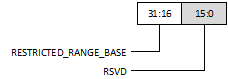
Bit |
Symbol |
Access |
Description |
|---|---|---|---|
31:16 |
RESTRICTED_RANGE_BASE |
R/W |
Indicates Way Restricted Range Base Address.(65536 bytes alignment) |
15:0 |
RSVD |
Reserved |
ICWRR_TOP
The ICWRR_TOP characteristics are:
Purpose: Provides Instruction Cache Way Restricted Range Top.
Usage constraints:
Privileged access permitted only. Unprivileged accesses generate a fault.
This register is word accessible only. Half-word and byte accesses are UNPREDICTABLE.
Attributes:
32-bit read/write register located at 0xE004_20A4.
This register can only be accessed from privileged request, and is RAZ/WI from Secure State if security extension presents.
Default value: 0xFFFF_0000
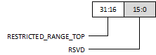
Bit |
Symbol |
Access |
Description |
|---|---|---|---|
31:16 |
RESTRICTED_RANGE_TOP |
R/W |
Indicates Way Restricted Range TOP Address.(65536 bytes alignment) |
15:0 |
RSVD |
Reserved |
DCWRR_BASE
The DCWRR_BASE characteristics are:
Purpose: Provides Data Cache Way Restricted Range base.
Usage constraints:
Privileged access permitted only. Unprivileged accesses generate a fault.
This register is word accessible only. Half-word and byte accesses are UNPREDICTABLE.
Attributes:
32-bit read/write register located at 0xE004_20A8.
This register can only be accessed from privileged request, and is RAZ/WI from Secure State if security extension presents.
Default value: 0x0000_0000

Bit |
Symbol |
Access |
Description |
|---|---|---|---|
31:16 |
RESTRICTED_RANGE_BASE |
R/W |
Indicates Way Restricted Range Base Address (65536 bytes alignment) |
15:0 |
RSVD |
Reserved |
DCWRR_TOP
The DCWRR_TOP characteristics are:
Purpose: Provides Data Cache Way Restricted Range Top.
Usage constraints:
Privileged access permitted only. Unprivileged accesses generate a fault.
This register is word accessible only. Half-word and byte accesses are UNPREDICTABLE.
Attributes:
32-bit read/write register located at 0xE004_20AC.
This register can only be accessed from privileged request, and is RAZ/WI from Secure State if security extension presents.
Defaultvalue: 0xFFFF_0000

Bit |
Symbol |
Access |
Description |
|---|---|---|---|
31:16 |
RESTRICTED_RANGE_TOP |
R/W |
Indicates Way Restricted Range TOP Address (65536 bytes alignment) |
15:0 |
RSVD |
Reserved |
DTCM0_BASE
The DTCM0_BASE characteristics are:
Purpose: Provides DTCM0 Range Base.
Usage constraints:
Privileged access permitted only. Unprivileged accesses generate a fault.
This register is word accessible only. Half-word and byte accesses are UNPREDICTABLE.
Attributes:
32-bit read/write register located at 0xE004_2060.
This register can only be accessed from privileged request, and is RAZ/WI from Secure State if security extension presents.
Default value: 0x0008_0000
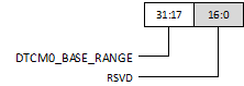
Bit |
Symbol |
Access |
Description |
|---|---|---|---|
31:17 |
DTCM0_BASE_RANGE |
R/W |
Indicates DTCM0 Range Base, aligned at 1K bytes. |
16:0 |
RSVD |
RO |
Reserved |
DTCM0_TOP
The DTCM0_TOP characteristics are:
Purpose: Provides DTCM0 Range Top.
Usage constraints:
Privileged access permitted only. Unprivileged accesses generate a fault.
This register is word accessible only. Half-word and byte accesses are UNPREDICTABLE.
Attributes:
32-bit read/write register located at 0xE004_2064.
This register can only be accessed from privileged request, and is RAZ/WI from Secure State if security extension presents.
Default value: 0x0009_7FFF
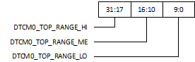
Bit |
Symbol |
Access |
Description |
|---|---|---|---|
31:17 |
DTCM0_TOP_RANGE_HI |
RO |
Higher bits of the DTCM0_TOP register. The value is the same with DTCM0_BASE[31:17]. |
16:10 |
DTCM0_TOP_RANGE_ME |
R/W |
Medium bits of the DTCM0_TOP register. The reset value is the bit[16:10] of the DTCM0_TOP register set in the configuration form. |
9:0 |
DTCM0_TOP_RANGE_LO |
RO |
Lower bits of the DTCM0_TOP register. The value is 10’h3ff. |